SBVS231A August   2014  – March 2015 TPS3847

PRODUCTION DATA.  

  1. Features
  2. Applications
  3. Description
  4. Revision History
  5. Pin Configuration and Functions
  6. Specifications
    1. 6.1 Absolute Maximum Ratings
    2. 6.2 ESD Ratings
    3. 6.3 Recommended Operating Conditions
    4. 6.4 Thermal Information
    5. 6.5 Electrical Characteristics
    6. 6.6 Timing Requirements
    7. 6.7 Typical Characteristics
  7. Detailed Description
    1. 7.1 Overview
    2. 7.2 Functional Block Diagram
    3. 7.3 Feature Description
      1. 7.3.1 Ultralow Supply Current
      2. 7.3.2 Wide Supply Range
      3. 7.3.3 High-Accuracy Negative Threshold
      4. 7.3.4 Push-Pull Output
      5. 7.3.5 Manual Reset (MR) Input
      6. 7.3.6 VCC Transient Rejection
      7. 7.3.7 Controlled Startup Current
      8. 7.3.8 Low Minimum Supply Voltage for Valid Output
    4. 7.4 Device Functional Modes
  8. Application and Implementation
    1. 8.1 Application Information
    2. 8.2 Typical Application
      1. 8.2.1 Design Requirements
        1. 8.2.1.1 Input Capacitor
        2. 8.2.1.2 Driving Bidirectional Reset Pins
        3. 8.2.1.3 Manual Reset (MR) Input
        4. 8.2.1.4 Threshold Overdrive
      2. 8.2.2 Detailed Design Procedure
      3. 8.2.3 Application Curves
    3. 8.3 Do's and Don'ts
  9. Power Supply Recommendations
  10. 10Layout
    1. 10.1 Layout Guidelines
    2. 10.2 Layout Example
  11. 11Device and Documentation Support
    1. 11.1 Device Support
      1. 11.1.1 Device Nomenclature
    2. 11.2 Documentation Support
      1. 11.2.1 Related Documentation
    3. 11.3 Trademarks
    4. 11.4 Electrostatic Discharge Caution
    5. 11.5 Glossary
  12. 12Mechanical, Packaging, and Orderable Information

Package Options

Mechanical Data (Package|Pins)
Thermal pad, mechanical data (Package|Pins)
Orderable Information

10 Layout

10.1 Layout Guidelines

Make sure the connection to the VCC pin is low impedance and able to carry 12 µA without a significant voltage drop. Place a 0.1-µF bypass capacitor near the VCC pin if the 12-µA current causes too much voltage droop.

10.2 Layout Example

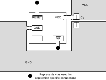
The layout example in Figure 20 shows how the TPS3847 is laid out on a printed circuit board (PCB). Although not required, use CIN for best device performance.
TPS3847 Layout_SBVS231.gifFigure 20. Layout Example