SBVS303B March 2017 – February 2018 TPS3890-Q1
PRODUCTION DATA.
- 1 Features
- 2 Applications
- 3 Description
- 4 Revision History
- 5 Device Comparison Table
- 6 Pin Configuration and Functions
- 7 Specifications
- 8 Detailed Description
- 9 Application and Implementation
- 10Power Supply Recommendations
- 11Layout
- 12Device and Documentation Support
- 13Mechanical, Packaging, and Orderable Information
Package Options
Mechanical Data (Package|Pins)
- DSE|6
Thermal pad, mechanical data (Package|Pins)
Orderable Information
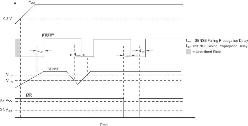
7.6 Timing Requirements
over the operating junction temperature range of –40°C to +125°C (TA = TJ), 1.5 V ≤ VDD ≤ 5.5 V, MR = VDD, and 5% input overdrive(1) (unless otherwise noted); typical values are at VDD = 5.5 V and TJ = 25°C| MIN | NOM | MAX | UNIT | |||
|---|---|---|---|---|---|---|
| tPD(f) | SENSE (falling) to RESET propagation delay | CT = open, VDD = 3.3 V | 18 | µs | ||
| CT = open, VDD = 5.5 V | 8 | |||||
| tPD(r) | SENSE (rising) to RESET propagation delay | CT = open, VDD = 3.3 V | 25 | µs | ||
| tGI(SENSE) | SENSE pin glitch immunity | VDD = 5.5 V | 9 | µs | ||
| tGI(MR) | MR pin glitch immunity | VDD = 5.5 V | 100 | ns | ||
| tMRW | MR pin pulse duration to assert RESET | 1 | µs | |||
| td(MR) | MR pin low to out delay | 250 | ns | |||
| tSTRT | Startup delay | 325 | µs | |||
(1) Overdrive = | (VIN / VTHRESH – 1) × 100% |.
 Figure 1. Timing Diagram