SLVSB16E November 2011 – December 2015 TPS43340-Q1
PRODUCTION DATA.
- 1 Features
- 2 Applications
- 3 Description
- 4 Revision History
- 5 Pin Configuration and Functions
- 6 Specifications
-
7 Detailed Description
- 7.1 Overview
- 7.2 Functional Block Diagram
- 7.3 Feature Description
- 7.4 Device Functional Modes
- 8 Application and Implementation
- 9 Power Supply Recommendations
- 10Layout
- 11Device and Documentation Support
- 12Mechanical, Packaging, and Orderable Information
Package Options
Mechanical Data (Package|Pins)
- PHP|48
Thermal pad, mechanical data (Package|Pins)
- PHP|48
Orderable Information
10 Layout
10.1 Layout Guidelines
Grounding and PCB Circuit Layout Considerations
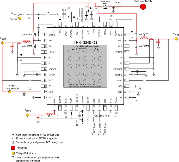
- Connect the drains of TOP_SW1 and TOP_SW2 together with the +ve terminal of the input capacitor COUT1. The trace length between these terminals should be short.
- The Kelvin-current sensing for the shunt resistor should have traces with minimum spacing, routed in parallel with each other. Place any filtering capacitors for noise near the IC pins.
- Connect the resistor divider for sensing output voltage between the +ve terminal of its respective output capacitor CBuck1 or CBuck2 or CBuck3 and the IC signal ground. Do not route these components or their traces near any switching nodes or high-current traces.
Other Considerations
- Separate the IC signal ground and power ground terminals (GND and PGNDx) pins. Use a star-ground configuration if connecting to a non-ground plane system. Use tie-ins for the EXTSUP capacitor, compensation network ground, and voltage-sense feedback ground networks to this star ground.
- Connect a compensation network between the compensation pins and IC signal ground. Connect the oscillator resistor (frequency setting) between the RT pin and IC signal ground. Do not locate these sensitive circuits near the dV/dt nodes; these include the gate drive outputs, phase pins, and boost circuits (bootstrap).
- Reduce the surface area of the high-current-carrying loops to a minimum by ensuring optimal component placement. Locate the bypass capacitors as close as possible to their respective power and ground pins.
10.3 Power Dissipation
The power dissipation depends on the MOSFET drive current and input voltage. The drive current is proportional to the total gate charge of the external MOSFET.
10.3.1 Power Dissipation of Buck1 and Buck2 (VOUT1 and VOUT2)
Assuming both high and low side MOSFETs are identical in a synchronous configuration, the total power dissipation per buck is
10.3.2 Power Dissipation of Buck Converter Buck3 (VOUT3)
10.3.2.1 High-Side Switch
The power dissipation losses are applicable for positive output currents:
10.3.2.2 Low-Side Switch
The power dissipation losses are applicable for positive output currents.
10.3.2.3 Linear Regulator (LREG1)
where
- VOUT = Output voltage, VIN = Input voltage
- IOUT = Output current, fSW = Switching frequency
- tr = Rise time of switching node PH3
- tf = Fall time of switching node PH3
- VREG = FET gate drive voltage
- Vf_diode = Low-side FET diode drop (conduction during dead time)
10.3.2.4 IC Power Consumption
Table 2. Summary of Equations for Component Selection(1)(2)
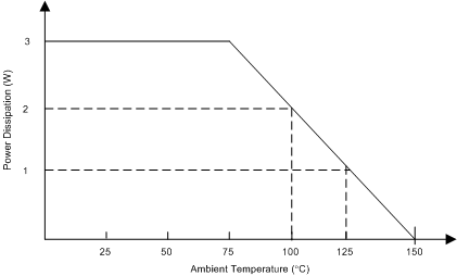
 Figure 24. Power Dissipation Derating Profile Based on High-K JEDEC PCB
10.4 Thermal Considerations
The TPS43340-Q1 is protected from overtemperature using an internal thermal shutdown circuit. If the die temperature exceeds the thermal shutdown threshold (for example, due to fault conditions such as a short circuit at the gate drivers or VREG), the device turns off, and restarts when the temperature has fallen by the hysteresis.
Table 3. Low-Power-Mode Operation of the System
| SETUP | SYNC | QUIESCENT CURRENT (TYP), NO LOAD, 25°C |
DESCRIPTION |
|---|---|---|---|
| Buck1 or Buck2 in LPM mode | Low | Approximately 30 µA | Configuration for ignition-off applications with standby functionality |
| Buck1 and Buck2 in LPM mode | Approximately 35 µA | ||
| Buck1 or Buck2 in PWM mode | High | Approximately 30-40 mA | Including switching currents |
| Buck1 and Buck2 in PWM mode | Approximately 30-40 mA | Including switching currents | |
| LREG1 | N/A | Approximately 50 µA | Configuration for ignition-off applications with standby functionality |
| LREG1 and Buck1 or Buck2 in LPM mode | Low | Approximately 55 µA | |
| LREG1 and Buck1 and Buck2 in LPM mode | Approximately 60 µA | ||
| LREG1 and Buck1 or Buck2 in PWM mode | High | 30-40 mA | Including switching currents |
| LREG1 and Buck1 and Buck2 in PWM mode | 30-40 mA | Including switching currents |
The synchronous buck converter Buck3 with the integrated FETs does not support LPM. Turning on Buck3 forces the system to operate in normal mode, and the quiescent current consumption increases.
Table 4. Input Voltage and Low-Power-Mode Operation
| INPUT VOLTAGE AT VIN PIN | LOAD CURRENT OF LREG1 | CHARGE PUMP OF LREG1 | BUCK CONTROLLERS Buck1 AND Buck2 |
VIN QUIESCENT CURRENT (TYP), NO LOAD, 25°C |
DESCRIPTION |
|---|---|---|---|---|---|
| VIN > 9 V | N/A | OFF | LPM allowed | 55 µA | Lowest current consumption of the system at VIN (LREG1, Buck1 and Buck2 enabled), typical ignition-off stay-alive mode with up to three voltage rails active |
| 7.5 V < VIN < 9 V | < 2 mA | OFF | LPM allowed | 55 µA | |
| > 6 mA | ON | LPM allowed | 260 µA | ||
| VIN < 7.5 V | N/A | ON | LPM not allowed | 2.6 mA | If VIN drops below 7.5 V, the buck controllers Buck1 and Buck2 leave low-power mode (LPM) and start PWM operation, quiescent current of the system increases. For applications that use the LREG1 only as the standby keep-alive supply, quiescent current is still low. |
Monitoring of the threshold for the charge pump of the low quiescent linear regulator LREG1 to be turned on occurs at the VIN pin. If using LREG1 as post regulator with an input voltage VLR1 of less than 7.5 V, the charge pump still stays off if operating within the required conditions for VIN and the load current. The sampling interval for the foregoing voltage thresholds at the VIN pin is typically 60 µs.
10.4.1 Phase Configuration
The IC configuration has buck controller 1 and buck controller 2 switching 180 degrees out of phase. Buck converter (Buck3) switches in phase with buck controller 1.
| CONFIGURATION | Buck1 | Buck2 | Buck3 | DESCRIPTION |
|---|---|---|---|---|
| Phase | 0º | 180º | 0º | Buck1 and Buck2 out of phase, Buck1 and Buck3 in phase |


