SLUSA48 June 2016 TPS51200-EP
PRODUCTION DATA.
- 1 Features
- 2 Applications
- 3 Description
- 4 Revision History
- 5 Pin Configuration and Functions
- 6 Specifications
-
7 Detailed Description
- 7.1 Overview
- 7.2 Functional Block Diagram
- 7.3
Feature Description
- 7.3.1 Sink and Source Regulator (VO Pin)
- 7.3.2 Reference Input (REFIN Pin)
- 7.3.3 Reference Output (REFOUT Pin)
- 7.3.4 Soft-Start Sequencing
- 7.3.5 Enable Control (EN Pin)
- 7.3.6 Powergood Function (PGOOD Pin)
- 7.3.7 Current Protection (VO Pin)
- 7.3.8 UVLO Protection (VIN Pin)
- 7.3.9 Thermal Shutdown
- 7.3.10 Tracking Start-up and Shutdown
- 7.4 Device Functional Modes
- 8 Application and Implementation
- 9 Power Supply Recommendations
- 10Layout
- 11Device and Documentation Support
- 12Mechanical, Packaging, and Orderable Information
Package Options
Mechanical Data (Package|Pins)
- DRC|10
Thermal pad, mechanical data (Package|Pins)
- DRC|10
Orderable Information
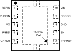
5 Pin Configuration and Functions
DRC Package
10-Pin VSON With Exposed Thermal Pad
Top View

Pin Functions
| PIN | I/O(2) | DESCRIPTION | |
|---|---|---|---|
| NAME | NO. | ||
| EN | 7 | I | For DDR VTT application, connect EN to SLP_S3. For any other application, use the EN pin as the ON/OFF function. |
| GND | 8 | G | Signal ground. Connect to negative terminal of the output capacitor. |
| PGND(1) | 4 | G | Power ground output for the LDO. |
| PGOOD | 9 | O | PGOOD output. Indicates regulation. |
| REFIN | 1 | I | Reference input. |
| REFOUT | 6 | O | Reference output. Connect to GND through 0.1-μF ceramic capacitor. |
| VIN | 10 | I | 2.5-V or 3.3-V power supply. A ceramic decoupling capacitor with a value between 1-μF and 4.7-μF is required. |
| VLDOIN | 2 | I | Supply voltage for the LDO. |
| VO | 3 | O | Power output for the LDO. |
| VOSNS | 5 | I | Voltage sense input for the LDO. Connect to positive terminal of the output capacitor or the load. |
(1) Thermal pad connection. See Figure 31 in the Thermal Design Considerations section for additional information.
(2) I = Input, O = Output, G = Ground.