SLUS909B May 2009 – August 2014 TPS53126
PRODUCTION DATA.
- 1 Features
- 2 Applications
- 3 Description
- 4 Simplified Schematics
- 5 Revision History
- 6 Pin Configurations and Functions
- 7 Specifications
-
8 Detailed Description
- 8.1 Overview
- 8.2 Functional Block Diagram
- 8.3
Feature Description
- 8.3.1 PWM Operation
- 8.3.2 Drivers
- 8.3.3 PWM Frequency And Adaptive On-time Control
- 8.3.4 5 Volt Regulator
- 8.3.5 Soft Start
- 8.3.6 Pre-Bias Support
- 8.3.7 Switching Frequency Selection
- 8.3.8 Output Discharge Control
- 8.3.9 Overcurrent Limit
- 8.3.10 Over/under Voltage Protection
- 8.3.11 UVLO Protection
- 8.3.12 Thermal Shutdown
- 8.4 Device Functional Modes
- 9 Application and Implementation
- 10Power Supply Recommendations
- 11Layout
- 12Device and Documentation Support
- 13Mechanical, Packaging, and Orderable Information
Package Options
Refer to the PDF data sheet for device specific package drawings
Mechanical Data (Package|Pins)
- RGE|24
- PW|24
Thermal pad, mechanical data (Package|Pins)
- RGE|24
Orderable Information
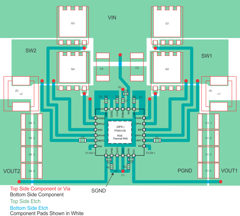
11 Layout
11.1 Layout Guidelines
- Keep the input switching current loop as small as possible. (VIN ≥ C3 ≥ PNGD ≥ Sync FET ≥ SW ≥ Control FET)
- Place the input capacitor (C3) close to the top switching FET. The output current loop should also be kept as small as possible.
- Keep the SW node as physically small and short as possible as to minimize parasitic capacitance and inductance and to minimize radiated emissions. Kelvin connections should be brought from the output to the feedback terminal (FBx) of the device.
- Keep analog and non-switching components away from switching components.
- Make a single point connection from the signal ground to power ground.(1)
- Do not allow switching current to flow under the device.
- DRVH and DRVL line should not run close to SW node or minimize it. (2)
- GND terminals for capacitors of SSx and V5FILT and resistors of feedback and TRIPx should be connected to SGND. (3)
- GND terminals for capacitors of VREG5 and VIN should be connected to PGND. (4)
- Signal lines should not run under/near Output Inductor or minimize it. (5)