SLUSB56B November 2012 – April 2019 TPS53819A
PRODUCTION DATA.
- 1 Features
- 2 Applications
- 3 Description
- 4 Revision History
- 5 Pin Configuration and Functions
- 6 Specifications
-
7 Detailed Description
- 7.1 Overview
- 7.2 Functional Block Diagram
- 7.3
Feature Description
- 7.3.1 Enable and Soft-Start
- 7.3.2 Adaptive On-Time Control
- 7.3.3 Zero Crossing Detection
- 7.3.4 Output Discharge Control
- 7.3.5 Low-Side Driver
- 7.3.6 High-Side Driver
- 7.3.7 Power Good
- 7.3.8 Current Sense and Overcurrent Protection
- 7.3.9 Overvoltage and Undervoltage Protection
- 7.3.10 Out-of-Bound Protection
- 7.3.11 UVLO Protection
- 7.3.12 Thermal Shutdown
- 7.4 Device Functional Modes
- 7.5 Programming
- 7.6
Register Maps
- 7.6.1 OPERATION [01h] (R/W Byte)
- 7.6.2 ON_OFF_CONFIG [02h] (R/W Byte)
- 7.6.3 WRITE_PROTECT [10h] (R/W Byte)
- 7.6.4 CLEAR_FAULTS [03h] (Send Byte)
- 7.6.5 STORE_DEFAULT_ALL [11h] (Send Byte)
- 7.6.6 RESTORE_DEFAULT_ALL [12h] (Send Byte)
- 7.6.7 STATUS_WORD [79h] (Read Word)
- 7.6.8 CUSTOM_REG (MFR_SPECIFIC_00) [D0h] (R/W Byte)
- 7.6.9 DELAY_CONTROL (MFR_SPECIFIC_01) [D1h] (R/W Byte)
- 7.6.10 MODE_SOFT_START_CONFIG (MFR_SPECIFIC_02) [D2h] (R/W Byte)
- 7.6.11 FREQUENCY_CONFIG (MFR_SPECIFIC_03) [D3h] (R/W Byte)
- 7.6.12 VOUT_ADJUSTMENT (MFR_SPECIFIC_04) [D4h] (R/W Byte)
- 7.6.13 Output Voltage Fine Adjustment Soft Slew Rate
- 7.6.14 VOUT_MARGIN (MFR_SPECIFIC_05) [D5h] (R/W Byte)
- 7.6.15 Output Voltage Margin Adjustment Soft-Slew Rate
- 7.6.16 UVLO_THRESHOLD (MFR_SPECIFIC_06) [D6h]
-
8 Application and Implementation
- 8.1 Application Information
- 8.2
Typical Application
- 8.2.1 Design Requirements
- 8.2.2
Detailed Design Procedure
- 8.2.2.1 Custom Design With WEBENCH® Tools
- 8.2.2.2 Switching Frequency
- 8.2.2.3 Inductor (L1)
- 8.2.2.4 Output Capacitors (C10, C11, C12, C13, C14)
- 8.2.2.5 Input Capacitors (C1, C2, C3, C4, C5)
- 8.2.2.6 MOSFET (Q1, Q2)
- 8.2.2.7 VREG Bypass Capacitor (C18)
- 8.2.2.8 VDD Bypass Capacitor (C19)
- 8.2.2.9 VBST Capacitor (C7)
- 8.2.2.10 Snubber (C8 and R9)
- 8.2.2.11 Feedback Resistance, RFBH and RFBL (R17 and R18)
- 8.2.2.12 Overcurrent Limit (OCL) Setting Resistance (R10)
- 8.2.2.13 PMBus Device Address (R3 and R4)
- 8.2.2.14 PGOOD Pullup Resistor (R2)
- 8.2.2.15 SCL and SDA Pulldown Resistors (R14 and R15)
- 8.2.2.16 PMBus Pullup Resistors
- 8.2.3 Application Curves
- 9 Power Supply Recommendations
- 10Layout
- 11Device and Documentation Support
- 12Mechanical, Packaging, and Orderable Information
Package Options
Mechanical Data (Package|Pins)
- RGT|16
Thermal pad, mechanical data (Package|Pins)
- RGT|16
Orderable Information
7.4.3 D-CAP2™ Mode
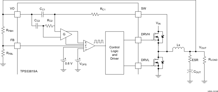
From small-signal loop analysis, a buck converter using D-CAP2™ mode control architecture can be simplified as shown in Figure 33.
 Figure 33. Simplified Modulator Using D-CAP2™ Control Architecture
 The D-CAP2 control architecture in TPS53819A includes an internal ripple generation network enabling the use of very low-ESR output capacitors such as multi-layer ceramic capacitors (MLCC). No external current sensing networks or compensators are required with D-CAP2 control architecture in order to simplify the power supply design. The role of the internal ripple generation network is to emulate the ripple component of the inductor current information and then combine it with the voltage feedback signal. VOFS is the internal offset to compensate the offset caused by the internal ripple, and the typical VOFS value is 4 mV. The 0-dB frequency of the D-CAP2 architecture can be approximated as shown in Equation 7.

where
- G is gain of the amplifier which amplifies the ripple current information generated by the network
- D is the duty ratio
The typical G value is 0.25. The RC1CC1 time constant value varies according to the selected switching frequency as shown in Table 1.
Table 1. Switching Frequency Selection
| SWITCHING FREQUENCY (kHz) | RC1CC1 TIME CONSTANT (µs) |
|---|---|
| 275 | 75 |
| 325 | |
| 425 | 62 |
| 525 | |
| 625 | 48 |
| 750 | |
| 850 | 36 |
| 1000 |
In order to secure enough phase margin, consider that f0 should be lower than 1/3 of the switching frequency, but is also higher than 5 times the fC2 as shown in Equation 8.

where
- fC2 is determined by the internal network of RC2 and CC2 (1.4 kHz typ)
This example describes a DC-DC converter with an input voltage range of 12-V and an output voltage of 1.2-V. If the switching frequency is 525 kHz and the inductor is given as 0.44uH, then COUT should be larger than 197 μF, and also be smaller than 4.9 mF based on the design requirements. The characteristics of the capacitors should be also taken into considerations. For MLCC, use X5R or better dielectric and take into account derating of the capacitance by both DC bias and AC bias. When derating by DC bias and AC bias are 80% and 50%, respectively, the effective derating is 40% because 0.8 x 0.5 = 0.4. The capacitance of specialty polymer capacitors may change depending on the operating frequency. Consult capacitor manufacturers for specific characteristics.