SLVSBM7A March 2013 – January 2016 TPS54061-Q1
PRODUCTION DATA.
- 1 Features
- 2 Applications
- 3 Description
- 4 Revision History
- 5 Pin Configuration and Functions
- 6 Specifications
-
7 Detailed Description
- 7.1 Overview
- 7.2 Functional Block Diagram
- 7.3
Feature Description
- 7.3.1 Fixed Frequency PWM Control
- 7.3.2 Slope Compensation Output Current
- 7.3.3 Error Amplifier
- 7.3.4 Voltage Reference
- 7.3.5 Adjusting the Output Voltage
- 7.3.6 Enable and Adjusting Undervoltage Lockout (UVLO)
- 7.3.7 Internal Slow-Start
- 7.3.8 Constant Switching Frequency and Timing Resistor (RT/CLK Pin)
- 7.3.9 Selecting the Switching Frequency
- 7.3.10 Synchronization to RT/CLK Pin
- 7.3.11 Overvoltage Protection
- 7.3.12 Thermal Shutdown
- 7.4 Device Functional Modes
-
8 Applications and Implementation
- 8.1 Application Information
- 8.2
Typical Applications
- 8.2.1
Continuous Conduction Mode Application
- 8.2.1.1 Design Requirements
- 8.2.1.2
Detailed Design Procedure
- 8.2.1.2.1 Selecting the Switching Frequency
- 8.2.1.2.2 Output Inductor Selection (LO)
- 8.2.1.2.3 Output Capacitor
- 8.2.1.2.4 Input Capacitor
- 8.2.1.2.5 Bootstrap Capacitor Selection
- 8.2.1.2.6 Undervoltage Lockout Set Point
- 8.2.1.2.7 Output Voltage and Feedback Resistors Selection
- 8.2.1.2.8 Closing the Loop
- 8.2.1.3 Application Curves
- 8.2.2 Discontinuous Conduction Mode Application
- 8.2.1
Continuous Conduction Mode Application
- 9 Power Supply Recommendations
- 10Layout
- 11Device and Documentation Support
- 12Mechanical, Packaging, and Orderable Information
Package Options
Mechanical Data (Package|Pins)
- DRB|8
Thermal pad, mechanical data (Package|Pins)
- DRB|8
Orderable Information
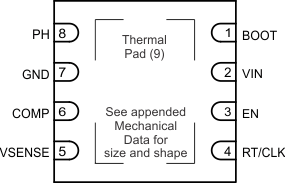
5 Pin Configuration and Functions
DRB Package
8-Pin SON
Bottom View

Pin Functions
| PIN | I/O | DESCRIPTION | |
|---|---|---|---|
| NO. | NAME | ||
| 1 | BOOT | O | The device requires a bootstrap capacitor between BOOT and PH. If the voltage on this capacitor is below the minimum required by the output device, the output switches off until refreshing of the capacitor is complete. |
| 2 | VIN | I | Input supply voltage, 4.7 V to 60 V |
| 3 | EN | I | Enable pin with internal pullup current source. Pull below 1.18 V to disable. Float to enable. Adjust the input undervoltage lockout (UVLO) with two resistors, see Enable and Adjusting Undervoltage Lockout. |
| 4 | RT/CLK | I | Resistor timing and external clock. An internal amplifier holds this pin at a fixed voltage when using an external resistor to ground to set the switching frequency. Pulling the pin above the PLL upper threshold causes a mode change, and the pin becomes a synchronization input. The change disables the internal amplifier, and the pin becomes a high-impedance clock input to the internal PLL. Stoppage of the clocking edges re-enables the internal amplifier, and the mode returns to a resistor frequency programming. |
| 5 | VSENSE | I | Inverting input of the transconductance (gm) error amplifier |
| 6 | COMP | O | Error amplifier output and input to the output switch current comparator. Connect frequency compensation components to this pin. |
| 7 | GND | G | Ground |
| 8 | PH | O | The source of the internal high-side power MOSFET and drain of the internal low-side MOSFET |
| 9 | Thermal pad | – | Connect the GND pin electrically to the exposed pad on the printed circuit board for proper operation. |