SLVSDG7A April 2016 – April 2021 TPS54202H
PRODUCTION DATA
- 1 Features
- 2 Applications
- 3 Description
- 4 Revision History
- 5 Pin Configuration and Functions
- 6 Specifications
-
7 Detailed Description
- 7.1 Overview
- 7.2 Functional Block Diagram
- 7.3
Feature Description
- 7.3.1 Fixed-Frequency PWM Control
- 7.3.2 Pulse Skip Mode
- 7.3.3 Error Amplifier
- 7.3.4 Slope Compensation and Output Current
- 7.3.5 Device Enable
- 7.3.6 Adjusting Under Voltage Lockout
- 7.3.7 Safe Startup into Pre-Biased Outputs
- 7.3.8 Voltage Reference
- 7.3.9 Adjusting Output Voltage
- 7.3.10 Internal Soft-Start
- 7.3.11 Bootstrap Voltage (BOOT)
- 7.3.12 Overcurrent Protection
- 7.3.13 Output Overvoltage Protection (OVP)
- 7.3.14 Thermal Shutdown
- 7.4 Device Functional Modes
- 8 Application and Implementation
- 9 Power Supply Recommendations
- 10Layout
- 11Device and Documentation Support
- 12Mechanical, Packaging, and Orderable Information
Package Options
Mechanical Data (Package|Pins)
- DDC|6
Thermal pad, mechanical data (Package|Pins)
Orderable Information
7.3.6 Adjusting Under Voltage Lockout
The device implements internal under voltage-lockout (UVLO) circuitry on the VIN pin. The device is disabled when the VIN pin voltage falls below the internal VIN UVLO threshold. The internal VIN UVLO threshold has a hysteresis of 480 mV. To enable the device, connect a pull-up resistor R4 (typical 510 KΩ to limit the quiescent current) to the VIN pin.
If an application requires a higher UVLO threshold on the VIN pin, then the EN pin can be configured as shown in Figure 7-1. When using the external UVLO function, setting the hysteresis at a value greater than 500 mV is recommended.
The EN pin has a pull-down resistance Rpd (typical 1 MΩ), which sets the default state of the pin to disable when no external components are connected. Use Equation 1 and Equation 2 to calculate the values of R4 and R5 for a specified UVLO threshold.
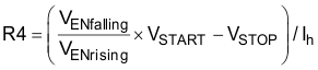
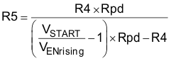
Where:
Ih = 1 µA
VENrising = 1.28 V
VENfalling = 1.25 V