SLUSCV2A June 2017 – April 2021 TPS54308
PRODUCTION DATA
- 1 Features
- 2 Applications
- 3 Description
- 4 Revision History
- 5 Pin Configuration and Functions
- 6 Specifications
-
7 Detailed Description
- 7.1 Overview
- 7.2 Functional Block Diagram
- 7.3
Feature Description
- 7.3.1 Fixed-Frequency PWM Control
- 7.3.2 Force Continuous Conduction Mode (FCCM)
- 7.3.3 Error Amplifier
- 7.3.4 Slope Compensation and Output Current
- 7.3.5 Enable and Adjusting Undervoltage Lockout
- 7.3.6 Safe Start-Up into Pre-Biased Outputs
- 7.3.7 Voltage Reference
- 7.3.8 Adjusting Output Voltage
- 7.3.9 Internal Soft Start
- 7.3.10 Bootstrap Voltage (BOOT)
- 7.3.11 Overcurrent Protection
- 7.3.12 Output Overvoltage Protection (OVP)
- 7.3.13 Thermal Shutdown
- 7.4 Device Functional Modes
-
8 Application and Implementation
- 8.1 Application Information
- 8.2
Typical Application
- 8.2.1 TPS54308 8-V to 28-V Input, 5-V Output Converter
- 8.2.2 Design Requirements
- 8.2.3 Detailed Design Procedure
- 8.2.4 Application Curves
- 9 Power Supply Recommendations
- 10Layout
- 11Device and Documentation Support
- 12Mechanical, Packaging, and Orderable Information
Package Options
Mechanical Data (Package|Pins)
- DDC|6
Thermal pad, mechanical data (Package|Pins)
Orderable Information
7.3.5 Enable and Adjusting Undervoltage Lockout
The EN pin provides electrical on and off control of the device. When the EN pin voltage exceeds the threshold voltage, the device begins operation. If the EN pin voltage is pulled below the threshold voltage, the regulator stops switching and enters the low-quiescent (IQ) state.
The EN pin has an internal pullup current source which allows the user to float the EN pin to enable the device. If an application requires control of the EN pin, use open-drain or open-collector output logic to interface with the pin.
The device implements internal undervoltage-lockout (UVLO) circuitry on the VIN pin. The device is disabled when the VIN pin voltage falls below the internal VIN UVLO threshold. The internal VIN UVLO threshold has a hysteresis of 480 mV.
If an application requires a higher UVLO threshold on the VIN pin, then the EN pin can be configured as shown in Figure 7-1. When using the external UVLO function, setting the hysteresis at a value greater than 500 mV is recommended.
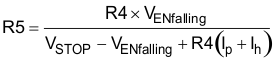
The EN pin has a small pullup current, Ip, which sets the default state of the pin to enable when no external components are connected. The pullup current is also used to control the voltage hysteresis for the UVLO function because it increases by Ih when the EN pin crosses the enable threshold. Use Equation 1 and Equation 2 to calculate the values of R4 and R5 for a specified UVLO threshold.
 Figure 7-1 Adjustable VIN Undervoltage Lockout
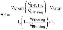
Where:
- Ip = 0.7 µA
- Ih = 1.55 µA
- VENfalling = 1.19 V
- VENrising = 1.22 V