SLVS416C February 2002 – January 2015 TPS54311 , TPS54312 , TPS54313 , TPS54314 , TPS54315 , TPS54316
PRODUCTION DATA.
- 1 Features
- 2 Applications
- 3 Description
- 4 Revision History
- 5 Pin Configuration and Functions
- 6 Specifications
-
7 Detailed Description
- 7.1 Overview
- 7.2 Functional Block Diagram
- 7.3
Feature Description
- 7.3.1 Undervoltage Lock Out (UVLO)
- 7.3.2 Slow-Start/Enable (SS/ENA)
- 7.3.3 VBIAS Regulator (VBIAS)
- 7.3.4 Voltage Reference
- 7.3.5 Oscillator and PWM Ramp
- 7.3.6 Error Amplifier
- 7.3.7 PWM Control
- 7.3.8 Dead-Time Control and MOSFET Drivers
- 7.3.9 Overcurrent Protection
- 7.3.10 Thermal Shutdown
- 7.3.11 Powergood (PWRGD)
- 7.4 Device Functional Modes
- 8 Application and Implementation
- 9 Power Supply Recommendations
- 10Layout
- 11Device and Documentation Support
- 12Mechanical, Packaging, and Orderable Information
Package Options
Mechanical Data (Package|Pins)
- PWP|20
Thermal pad, mechanical data (Package|Pins)
- PWP|20
Orderable Information
6 Specifications
6.1 Absolute Maximum Ratings
over operating free-air temperature range (unless otherwise noted)(1)| MIN | MAX | UNIT | |||
|---|---|---|---|---|---|
| VI | Input voltage | VIN, SS/ENA, SYNC | −0.3 | 7 | V |
| RT | −0.3 | 6 | V | ||
| VSENSE | −0.3 | 4 | V | ||
| BOOT | −0.3 | 17 | V | ||
| VO | Output voltage | VBIAS, PWRGD, COMP | −0.3 | 7 | V |
| PH | −0.6 | 10 | V | ||
| IO | Source current | PH | Internally Limited | V | |
| COMP, VBIAS | 6 | mA | |||
| IS | Sink current | PH | 6 | A | |
| COMP | 6 | mA | |||
| SS/ENA, PWRGD | 10 | mA | |||
| Voltage differential | AGND to PGND | ±0.3 | V | ||
| TJ | Operating virtual junction temperature | –40 | 125 | °C | |
| Tstg | Storage temperature | −65 | 150 | °C | |
(1) Stresses beyond those listed under Absolute Maximum Ratings may cause permanent damage to the device. These are stress ratings only, which do not imply functional operation of the device at these or any other conditions beyond those indicated under Recommended Operating Conditions. Exposure to absolute-maximum-rated conditions for extended periods may affect device reliability.
6.2 Recommended Operating Conditions
over operating free-air temperature range (unless otherwise noted)| MIN | MAX | UNIT | ||
|---|---|---|---|---|
| VI | Input voltage range | 3 | 6 | V |
| TJ | Operating junction temperature | –40 | 125 | °C |
6.3 Thermal Information(2)
| THERMAL METRIC(1) | TPS5431x | UNIT | |
|---|---|---|---|
| PWP (28 PINS) | |||
| RθJA | Junction-to-ambient thermal resistance | 26.0 | °C/W |
| Junction-to-ambient thermal resistance (without solder on PowerPad) | 57.5 | ||
(1) For more information about traditional and new thermal metrics, see the IC Package Thermal Metrics application report, SPRA953.
(2) Test board conditions:
- 3 inches × 3 inches, 2 layers, Thickness 0.062 inch
- 1.5 oz copper traces located on the top of the PCB
- 1.5 oz copper plane on the bottom of the PCB
- Ten thermal vias (see recommended land pattern)
6.4 Dissipation Ratings(1)(2)
| PACKAGE | TA = 25 °C POWER RATING |
TA = 70 °C POWER RATING |
TA = 85 °C POWER RATING |
UNIT |
|---|---|---|---|---|
| 20-Pin PWP with solder | 3.85(3) | 2.12 | 1.54 | W |
| 20-pin PWP without solder | 1.73 | 0.96 | 0.69 | W |
(1) For more information on the PWP package, refer to TI technical brief, SLMA002
(2) Test board conditions:
- 3 inches × 3 inches, 2 layers, Thickness 0.062 inch
- 1.5 oz copper traces located on the top of the PCB
- 1.5 oz copper plane on the bottom of the PCB
- Ten thermal vias (see recommended land pattern)
(3) Maximum power dissipation may be limited by overcurrent protection
6.5 Electrical Characteristics
TJ = –40°C to 125°C, VIN = 3 V to 6 V (unless otherwise noted)| PARAMETER | TEST CONDITIONS | MIN | TYP | MAX | UNIT | ||
|---|---|---|---|---|---|---|---|
| SUPPLY VOLTAGE, VIN | |||||||
| VIN | Input voltage range | 3 | 6 | V | |||
| I(Q) | Quiescent current | fs = 350 kHz, FSEL ≤ 0.8 V, RT open | 6.2 | 9.6 | mA | ||
| fs = 550 kHz, FSEL ≤ 2.5 V, RT open, Phase pin open | 8.4 | 12.8 | |||||
| Shutdown, SS/ENA = 0 V | 1 | 1.4 | |||||
| UNDERVOLTAGE LOCK OUT | |||||||
| UVLO | Start threshold voltage | 2.95 | 3.0 | V | |||
| Stop threshold voltage | 2.70 | 2.80 | V | ||||
| Hysteresis voltage | 0.14 | 0.16 | V | ||||
| Rising and falling edge deglitch (1) | 2.5 | µs | |||||
| BIAS VOLTAGE | |||||||
| VBIAS | Output voltage | I(VBIAS) = 0 | 2.70 | 2.80 | 2.90 | V | |
| Output current(2) | 100 | µA | |||||
| OUTPUT VOLTAGE | |||||||
| VO | Output voltage | TPS54311 | TJ = 25°C, VIN = 5 V | 0.9 | V | ||
| 3 V ≤ VIN ≤ 6 V, 0 ≤ IL ≤ 3 A, −40°C ≤ TJ ≤ 125°C | –2.5% | 2.5% | |||||
| TPS54312 | TJ = 25°C, VIN = 5 V | 1.2 | V | ||||
| 3 V ≤ VIN ≤ 6 V, 0 ≤ IL ≤ 3 A, −40°C ≤ TJ ≤ 125°C | –2.5% | 2.5% | |||||
| TPS54313 | TJ = 25°C, VIN = 5 V | 1.5 | V | ||||
| 3 V ≤ VIN ≤ 6 V, 0 ≤ IL ≤ 3 A, −40°C ≤ TJ ≤ 125°C | –2.5% | 2.5% | |||||
| TPS54314 | TJ = 25°C, VIN = 5 V | 1.8 | V | ||||
| 3 V ≤ VIN ≤ 6 V, 0 ≤ IL ≤ 3 A, −40°C ≤ TJ ≤ 125°C | –2.5% | 2.5% | |||||
| TPS54315 | TJ = 25°C, VIN = 5 V | 2.5 | V | ||||
| 3 V ≤ VIN ≤ 6 V, 0 ≤ IL ≤ 3 A, −40° ≤ TJ ≤ 125°C | –2.5% | 2.5% | |||||
| TPS54316 | TJ = 25°C, VIN = 5 V | 3.3 | V | ||||
| 4 V ≤ VIN ≤ 6 V, 0 ≤ IL ≤ 3 A, −40° ≤ TJ ≤ 125°C | −2.5% | 2.5% | |||||
| REGULATION | |||||||
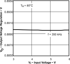
| Line regulation(1)(3) | IL = 3 A, 350 ≤ fs ≤ 550 kHz, TJ = 85°C | 0.21 | %/V | ||||
| Load regulation(1)(3) | IL = 0 A to 3 A, 350 ≤ fs ≤ 550 kHz, TJ = 85°C | 0.21 | %/A | ||||
| OSCILLATOR | |||||||
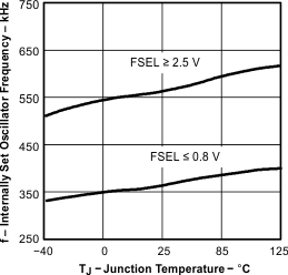
| Internally set-free running frequency | FSEL ≤ 0.8 V, RT open | 280 | 350 | 420 | kHz | ||
| FSEL ≥ 2.5 V, RT open | 440 | 550 | 660 | ||||
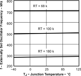
| Externally set-free running frequency range | RT = 180 kΩ (1% resistor to AGND)(1) | 252 | 280 | 308 | kHz | ||
| RT = 100 kΩ (1% resistor to AGND) | 460 | 500 | 540 | ||||
| RT = 68 kΩ (1% resistor to AGND)(1) | 663 | 700 | 762 | ||||
| High level threshold voltage at FSEL | 2.5 | V | |||||
| Low level threshold voltage at FSEL | 0.8 | V | |||||
| Ramp valley(1) | 0.75 | V | |||||
| Ramp amplitude (peak-to-peak)(1) | 1 | V | |||||
| Minimum controllable on time(1) | 200 | ns | |||||
| Maximum duty cycle(1) | 90% | ||||||
| ERROR AMPLIFIER | |||||||
| Error amplifier open loop voltage gain(4) | 26 | dB | |||||
| Error amplifier unity gain bandwidth(4) | 3 | 5 | MHz | ||||
| PWM COMPARATOR | |||||||
| PWM comparator propagation delay time, PWM comparator input to PH pin (excluding dead time) | 10-mV overdrive(4) | 70 | 85 | ns | |||
| SLOW-START/ENABLE | |||||||
| Enable threshold voltage, SS/ENA | 0.82 | 1.20 | 1.40 | V | |||
| Enable hysteresis voltage, SS/ENA(4) | 0.03 | V | |||||
| Falling edge deglitch, SS/ENA(4) | 2.5 | µs | |||||
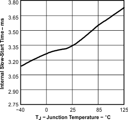
| Internal slow-start time(4) | TPS54311 | 2.6 | 3.3 | 4.1 | ms | ||
| TPS54312 | 3.5 | 4.5 | 5.4 | ||||
| TPS54313 | 4.4 | 5.6 | 6.7 | ||||
| TPS54314 | 2.6 | 3.3 | 4.1 | ||||
| TPS54315 | 3.6 | 4.7 | 5.6 | ||||
| TPS54316 | 4.7 | 6.1 | 7.6 | ||||
| Charge current, SS/ENA | SS/ENA = 0V | 3 | 5 | 8 | µA | ||
| Discharge current, SS/ENA | SS/ENA = 0.2 V, VI = 1.5 V | 1.5 | 2.3 | 4 | mA | ||
| POWERGOOD | |||||||
| Powergood threshold voltage | VSENSE falling | 90 | %Vref | ||||
| Powergood hysteresis voltage(4) | 3 | %Vref | |||||
| Powergood falling edge deglitch(4) | 35 | µs | |||||
| Output saturation voltage, PWRGD | I(sink) = 2.5 mA | 0.18 | 0.30 | V | |||
| Leakage current, PWRGD | VI = 5.5 V | 1 | µA | ||||
| CURRENT LIMIT | |||||||
| Current limit | VI = 3 V, output shorted(4) | 42 | 6.5 | A | |||
| VI = 6 V, output shorted(4) | 4.5 | 7.5 | |||||
| Current limit leading edge blanking time(4) | 100 | ns | |||||
| Current limit total response time(4) | 200 | ns | |||||
| THERMAL SHUTDOWN | |||||||
| Thermal shutdown trip point(4) | 135 | 150 | 165 | °C | |||
| Thermal shutdown hysteresis(4) | 10 | ||||||
| OUTPUT POWER MOSFETS | |||||||
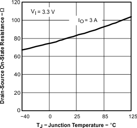
| rDS(on) | Power MOSFET switches | VI = 6 V(5) | 59 | 88 | mΩ | ||
| IO = 3 A, VI = 3 V(5) | 856 | 136 | |||||
(1) Specified by design
(2) Static resistive loads only
(3) Specified by the circuit used in Figure 10.
(4) Specified by design
(5) Matched MOSFETs, low side rDS(on) production tested, high side rDS(on) specified by design.
6.6 Typical Characteristics
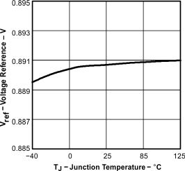
vs Junction Temperature
vs Junction Temperature
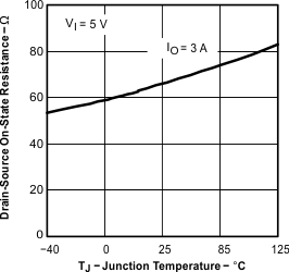
vs Junction Temperature
vs Junction Temperature