SLUSCK3 July 2016 TPS54335-2A
PRODUCTION DATA.
- 1 Features
- 2 Applications
- 3 Description
- 4 Revision History
- 5 Pin Configuration and Functions
- 6 Specifications
-
7 Detailed Description
- 7.1 Overview
- 7.2 Functional Block Diagram
- 7.3
Feature Description
- 7.3.1 Fixed-Frequency PWM Control
- 7.3.2 Light-Load Operation
- 7.3.3 Voltage Reference
- 7.3.4 Adjusting the Output Voltage
- 7.3.5 Enabling and Adjusting Undervoltage Lockout
- 7.3.6 Error Amplifier
- 7.3.7 Slope Compensation and Output Current
- 7.3.8 Safe Startup into Pre-Biased Outputs
- 7.3.9 Bootstrap Voltage (BOOT)
- 7.3.10 Output Overvoltage Protection (OVP)
- 7.3.11 Overcurrent Protection
- 7.3.12 Thermal Shutdown
- 7.3.13 Small-Signal Model for Loop Response
- 7.3.14 Simple Small-Signal Model for Peak Current-Mode Control
- 7.3.15 Small-Signal Model for Frequency Compensation
- 7.4 Device Functional Modes
-
8 Application and Implementation
- 8.1 Application Information
- 8.2
Typical Applications
- 8.2.1 Design Requirements
- 8.2.2 Detailed Design Procedure
- 8.2.3 Application Curves
- 9 Power Supply Recommendations
- 10Layout
- 11Device and Documentation Support
- 12Mechanical, Packaging, and Orderable Information
Package Options
Mechanical Data (Package|Pins)
- DRC|10
Thermal pad, mechanical data (Package|Pins)
- DRC|10
Orderable Information
8 Application and Implementation
NOTE
Information in the following applications sections is not part of the TI component specification, and TI does not warrant its accuracy or completeness. TI’s customers are responsible for determining suitability of components for their purposes. Customers should validate and test their design implementation to confirm system functionality.
8.1 Application Information
The TPS54335-2A family of devices are step-down DC-DC converters. The devices are typically used to convert a higher DC voltage to a lower DC voltage with a maximum available output current of 3 A. Use the following design procedure to select component values for each device. Alternately, use the WEBENCH software to generate a complete design. The WEBENCH software uses an iterative design procedure and accesses a comprehensive database of components when generating a design. This section presents a simplified discussion of the design process.
8.1.1 Supplementary Guidance
The device must operate within 150°C to ensure continuous function and operation of the device.
8.1.2 The DRC Package
The TPS54335-2A device is packaged in the a 3-mm × 3-mm SON package which is designated as DRC (see the Mechanical, Packaging, and Orderable Information section for all package options).
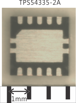 Figure 20. TPS54335-2A DRC Package
8.2 Typical Applications
TPS54335-2A typical application.
 Figure 21. Typical Application Schematic, TPS54335-2A
8.2.1 Design Requirements
For this design example, use the parameters listed in Table 1.
Table 1. Design Parameters
| DESIGN PARAMETER | EXAMPLE VALUE |
|---|---|
| Input voltage range | 8 to 28 V |
| Output voltage | 5 V |
| Transient response, 1.5-A load step | ΔVO = ±5 % |
| Input ripple voltage | 400 mV |
| Output ripple voltage | 30 mV |
| Output current rating | 3 A |
| Operating Frequency | 340 kHz |
8.2.2 Detailed Design Procedure
The following design procedure can be used to select component values for the TPS54335-2A device. Alternately, the WEBENCH® software may be used to generate a complete design. The WEBENCH software uses an iterative design procedure and accesses a comprehensive database of components when generating a design. This section presents a simplified discussion of the design process using the TPS54335-2A device.
For this design example, use the input parameters listed in Table 1.
8.2.2.1 Switching Frequency
Use to calculate the required value for R7. The calculated value is 140.6 kΩ. Use the next higher standard value of 143 kΩ for R7.
8.2.2.2 Output Voltage Set Point
The output voltage of the TPS54335-2A device is externally adjustable using a resistor divider network. In the application circuit of , this divider network is comprised of R5 and R6. Use Equation 13 and Equation 14 to calculate the relationship of the output voltage to the resistor divider.


Select a value of R5 to be approximately 100 kΩ. Slightly increasing or decreasing R5 can result in closer output-voltage matching when using standard value resistors. In this design, R5 = 100 kΩ and R6 = 19.1 kΩ which results in a 4.988-V output voltage. The 51.1-Ω resistor, R4, is provided as a convenient location to break the control loop for stability testing.
8.2.2.3 Undervoltage Lockout Set Point
The undervoltage lockout (UVLO) set point can be adjusted using the external-voltage divider network of R1 and R2. R1 is connected between the VIN and EN pins of the TPS54335-2A device. R2 is connected between the EN and GND pins. The UVLO has two thresholds, one for power up when the input voltage is rising and one for power down or brown outs when the input voltage is falling. For the example design, the minimum input voltage is 8 V, so the start-voltage threshold is set to 7.15 V with 1-V hysteresis. Use Equation 2 and Equation 3 to calculate the values for the upper and lower resistor values of R1 and R2.
8.2.2.4 Input Capacitors
The TPS54335-2A device requires an input decoupling capacitor and, depending on the application, a bulk input capacitor. The typical recommended value for the decoupling capacitor is 10 μF. A high-quality ceramic type X5R or X7R is recommended. The voltage rating should be greater than the maximum input voltage. A smaller value can be used as long as all other requirements are met; however a 10-μF capacitor has been shown to work well in a wide variety of circuits. Additionally, some bulk capacitance may be needed, especially if the TPS54335-2A circuit is not located within about 2 inches from the input voltage source. The value for this capacitor is not critical but should be rated to handle the maximum input voltage including ripple voltage, and should filter the output so that input ripple voltage is acceptable. For this design, a 10-μF, X7R dielectric capacitor rated for 35 V is used for the input decoupling capacitor. The ESR is approximately 2 mΩ, and the current rating is 3 A. Additionally, a small 0.1-μF capacitor is included for high frequency filtering.
Use Equation 15 to calculate the input ripple voltage (ΔVIN).

where
- CBULK is the bulk capacitor value
- ƒSW is the switching frequency
- IOUT(MAX) is the maximum load current
- ESRMAX is the maximum series resistance of the bulk capacitor
The maximum RMS (root mean square) ripple current must also be checked. For worst case conditions, use Equation 16 to calculate ICIN(RMS).

In this case, the input ripple voltage is 227 mV and the RMS ripple current is 1.5 A.
NOTE
The actual input-voltage ripple is greatly affected by parasitics associated with the layout and the output impedance of the voltage source.
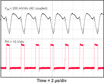
The Design Requirements section shows the actual input voltage ripple for this circuit which is larger than the calculated value. This measured value is still below the specified input limit of 400 mV. The maximum voltage across the input capacitors is VIN(MAX) + ΔVIN / 2. The selected bypass capacitor is rated for 35 V and the ripple current capacity is greater than 3 A. Both values provide ample margin. The maximum ratings for voltage and current must not be exceeded under any circumstance.
8.2.2.5 Output Filter Components
Two components must be selected for the output filter, the output inductor (LO) and CO. Because the TPS54335-2A device is an externally compensated device, a wide range of filter component types and values can be supported.
8.2.2.5.1 Inductor Selection
Use Equation 17 to calculate the minimum value of the output inductor (LMIN).

where
- KIND is a coefficient that represents the amount of inductor ripple current relative to the maximum output current
In general, the value of KIND is at the discretion of the designer; however, the following guidelines may be used. For designs using low-ESR output capacitors, such as ceramics, a value as high as KIND = 0.3 can be used. When using higher ESR output capacitors, KIND = 0.2 yields better results.
For this design example, use KIND = 0.3. The minimum inductor value is calculated as 13.4 μH. For this design, a close standard value of 15 µH was selected for LMIN.
For the output filter inductor, the RMS current and saturation current ratings must not be exceeded. Use Equation 18 to calculate the RMS inductor current (IL(RMS)).

Use Equation 19 to calculate the peak inductor current (IL(PK)).

For this design, the RMS inductor current is 3.002 A and the peak inductor current is 3.503 A. The selected inductor is a Coilcraft 15 μH, XAL6060-153MEB. This inductor has a saturation current rating of 5.8 A and an RMS current rating of 6 A which meets the requirements. Smaller or larger inductor values can be used depending on the amount of ripple current the designer wants to allow so long as the other design requirements are met. Larger value inductors have lower AC current and result in lower output voltage ripple. Smaller inductor values increase AC current and output voltage ripple. In general, for the TPS54335-2A device, use inductors with values in the range of 0.68 μH to 100 μH.
8.2.2.5.2 Capacitor Selection
Consider three primary factors when selecting the value of the output capacitor. The output capacitor determines the modulator pole, the output voltage ripple, and how the regulator responds to a large change in load current. The output capacitance must be selected based on the more stringent of these three criteria.
The desired response to a large change in the load current is the first criterion. The output capacitor must supply the load with current when the regulator cannot. This situation occurs if the desired hold-up times are present for the regulator. In this case, the output capacitor must hold the output voltage above a certain level for a specified amount of time after the input power is removed. The regulator is also temporarily unable to supply sufficient output current if a large, fast increase occurs affecting the current requirements of the load, such as a transition from no load to full load. The regulator usually requires two or more clock cycles for the control loop to notice the change in load current and output voltage and to adjust the duty cycle to react to the change. The output capacitor must be sized to supply the extra current to the load until the control loop responds to the load change. The output capacitance must be large enough to supply the difference in current for 2 clock cycles while only allowing a tolerable amount of drop in the output voltage. Use Equation 20 to calculate the minimum required output capacitance.

where
- ΔIOUT is the change in output current
- ƒSW is the switching frequency of the regulator
- ΔVOUT is the allowable change in the output voltage
For this example, the transient load response is specified as a 5% change in the output voltage, VOUT, for a load step of 1.5 A. For this example, ΔIOUT = 1.5 A and ΔVOUT = 0.05 × 5 = 0.25 V. Using these values results in a minimum capacitance of 35.3 μF. This value does not consider the ESR of the output capacitor in the output voltage change. For ceramic capacitors, the ESR is usually small enough to ignore in this calculation.
Equation 21 calculates the minimum output capacitance required to meet the output voltage ripple specification. In this case, the maximum output voltage ripple is 30 mV. Under this requirement, Equation 21 yields 12.3 µF.

where
- ƒSW is the switching frequency
- VOUTripple is the maximum allowable output voltage ripple
- Iripple is the inductor ripple current
Use Equation 22 to calculate the maximum ESR an output capacitor can have to meet the output-voltage ripple specification. Equation 22 indicates the ESR should be less than 29.8 mΩ. In this case, the ESR of the ceramic capacitor is much smaller than 29.8 mΩ.

Additional capacitance deratings for aging, temperature, and DC bias should be considered which increases this minimum value. For this example, two 47-μF 10-V X5R ceramic capacitors with 3 mΩ of ESR are used. Capacitors generally have limits to the amount of ripple current they can handle without failing or producing excess heat. An output capacitor that can support the inductor ripple current must be specified. Some capacitor data sheets specify the RMS value of the maximum ripple current. Use Equation 23 to calculate the RMS ripple current that the output capacitor must support. For this application, Equation 23 yields 116.2 mA for each capacitor.

8.2.2.6 Compensation Components
Several possible methods exist to design closed loop compensation for DC-DC converters. For the ideal current-mode control, the design equations can be easily simplified. The power stage gain is constant at low frequencies, and rolls off at –20 dB/decade above the modulator pole frequency. The power stage phase is 0 degrees at low frequencies and begins to fall one decade below the modulator pole frequency reaching a minimum of –90 degrees which is one decade above the modulator pole frequency. Use Equation 24 to calculate the simple modulator pole (ƒp_mod).

For the TPS54335-2A device, most circuits have relatively high amounts of slope compensation. As more slope compensation is applied, the power stage characteristics deviate from the ideal approximations. The phase loss of the power stage will now approach –180 degrees, making compensation more difficult. The power stage transfer function can be solved but it requires a tedious calculation. Use the PSpice model to accurately model the power-stage gain and phase so that a reliable compensation circuit can be designed. Alternately, a direct measurement of the power stage characteristics can be used which is the technique used in this design procedure. For this design, the calculated values are as follows:
L1 = 15 µH
C6 and C7 = 47 µF
ESR = 3 mΩ
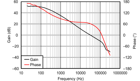
Figure 22 shows the power stage characteristics.
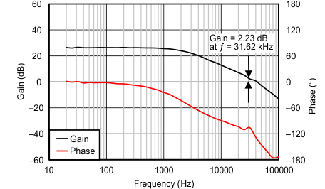 Figure 22. Power Stage Gain and Phase Characteristics
For this design, the intended crossover frequency is 31.62 kHz (an actual measured data point exists for that frequency). From the power stage gain and phase plots, the gain at 31.62 kHz is 2.23 dB and the phase is about -106 degrees. For 60 degrees of phase margin, additional phase boost from a feed-forward capacitor in parallel with the upper resistor of the voltage set point divider is not needed. R3 sets the gain of the compensated error amplifier to be equal and opposite the power stage gain at crossover. Use Equation 25 to calculate the required value of R3.

To maximize phase gain, the compensator zero is placed one decade below the crossover frequency of 31.62 kHz. Use Equation 26 to calculate the required value for C4.

To maximize phase gain the high frequency pole is placed one decade above the crossover frequency of 31.62 kHz. The pole can also be useful to offset the ESR of aluminum electrolytic output capacitors. Use Equation 27 to calculate the value of C5.

For this design the calculated values for the compensation components are as follows:
R3 = 3.74 kΩ
C4 = 0.012 µF
C5 = 120 pF
8.2.2.7 Bootstrap Capacitor
Every TPS54335-2A design requires a bootstrap capacitor, C3. The bootstrap capacitor value must 0.1 μF. The bootstrap capacitor is located between the PH and BOOT pins. The bootstrap capacitor should be a high-quality ceramic type with X7R or X5R grade dielectric for temperature stability.
8.2.2.8 Power Dissipation Estimate
The following formulas show how to estimate the device power dissipation under continuous-conduction mode operations. These formulas should not be used if the device is working in the discontinuous conduction mode (DCM) or pulse-skipping Eco-mode™.
The device power dissipation includes:
- Conduction loss:
- IOUT is the output current (A)
- rDS(on) is the on-resistance of the high-side MOSFET (Ω)
- VOUT is the output voltage (V)
- VIN is the input voltage (V)
- Switching loss:
- ƒSW is the switching frequency (Hz)
- Gate charge loss:
- Quiescent current loss:
where
where
Therefore:
where
- Ptot is the total device power dissipation (W)
For given TA :
where
- TA is the ambient temperature (°C)
- TJ is the junction temperature (°C)
- Rth is the thermal resistance of the package (°C/W)
For given TJ = 150°C:
where
- TAmax is the maximum ambient temperature (°C)
- TJmax is the maximum junction temperature (°C)
8.2.3 Application Curves
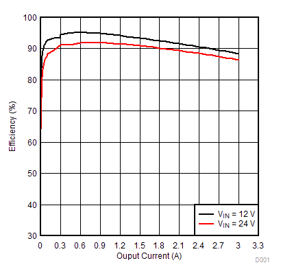
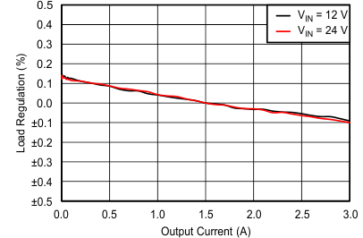
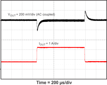
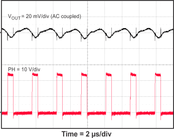
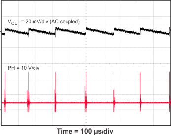
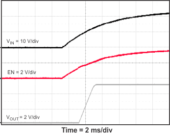
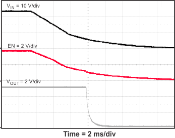
| 0.75- to 2.25-A load step | Slew rate = 500 mA/µs |
