SLUS774C AUGUST 2007 – December 2014 TPS54383 , TPS54386
PRODUCTION DATA.
- 1 Features
- 2 Applications
- 3 Description
- 4 Revision History
- 5 Pin Configuration and Functions
- 6 Specifications
-
7 Detailed Description
- 7.1 Overview
- 7.2 Functional Block Diagram
- 7.3
Feature Description
- 7.3.1 Voltage Reference
- 7.3.2 Oscillator
- 7.3.3 Input Undervoltage Lockout (UVLO) and Startup
- 7.3.4 Enable and Timed Turn On of the Outputs
- 7.3.5 Output Voltage Sequencing
- 7.3.6 Soft-Start
- 7.3.7 Output Voltage Regulation
- 7.3.8 Feedback Loop and Inductor-Capacitor (L-C) Filter Selection
- 7.3.9 Inductor-Capacitor (L-C) Selection
- 7.3.10 Maximum Output Capacitance
- 7.3.11 Minimum Output Capacitance
- 7.3.12 Modifying The Feedback Loop
- 7.3.13 Example: TPS54386 Buck Converter Operating at 12-V Input, 3.3-V Output and 400-mA(P-P) Ripple Current
- 7.3.14 Bootstrap for the N-Channel MOSFET
- 7.3.15 Light Load Operation
- 7.3.16 SW Node Ringing
- 7.3.17 Output Overload Protection
- 7.3.18 Operating Near Maximum Duty Cycle
- 7.3.19 Dual Supply Operation
- 7.3.20 Cascading Supply Operation
- 7.3.21 Multiphase Operation
- 7.3.22 Bypass and FIltering
- 7.3.23 Overtemperature Protection and Junction Temperature Rise
- 7.3.24 Power Derating
- 7.4 Device Functional Modes
-
8 Applications and Implementation
- 8.1 Application Information
- 8.2
Typical Applications
- 8.2.1
12-V to 5-V and 3.3-V Converter
- 8.2.1.1 Design Requirements
- 8.2.1.2
Detailed Design Procedure
- 8.2.1.2.1 Duty Cycle Estimation
- 8.2.1.2.2 Inductor Selection
- 8.2.1.2.3 Rectifier Diode Selection
- 8.2.1.2.4 Output Capacitor Selection
- 8.2.1.2.5 Voltage Setting
- 8.2.1.2.6 Compensation Capacitors
- 8.2.1.2.7 Input Capacitor Selection
- 8.2.1.2.8 Boot Strap Capacitor
- 8.2.1.2.9 ILIM
- 8.2.1.2.10 SEQ
- 8.2.1.2.11 Power Dissipation
- 8.2.1.3 Application Curves
- 8.2.2 24-V to 12-V and 24-V to 5-V
- 8.2.3 5-V to 3.3V and 5-V to 1.2 V
- 8.2.1
12-V to 5-V and 3.3-V Converter
- 9 Power Supply Recommendations
- 10Layout
- 11Device and Documentation Support
- 12Mechanical, Packaging, and Orderable Information
Package Options
Refer to the PDF data sheet for device specific package drawings
Mechanical Data (Package|Pins)
- PWP|14
Thermal pad, mechanical data (Package|Pins)
- PWP|14
Orderable Information
6 Specifications
6.1 Absolute Maximum Ratings(1)
| MIN | MAX | UNIT | ||
|---|---|---|---|---|
| Input voltage range | PVDD1, PVDD2, EN1, EN2 | 30 | V | |
| BOOT1, BOOT2 | VSW+ 7 | |||
| SW1, SW2 | –2 | 30 | ||
| SW1, SW2 transient (< 50ns) | –3 | 31 | ||
| BP | 6.5 | |||
| SEQ, ILIM2 | –0.3 | 6.5 | ||
| FB1, FB2 | –0.3 | 3 | ||
| SW1, SW2 output current | 7 | A | ||
| BP load current | 35 | mA | ||
| TJ | Operating temperature | –40 | +150 | °C |
| Soldering temperature | +260 | |||
| Tstg | Storage temperature | –55 | 165 | °C |
(1) Permanent device damage may occur if Absolute Maximum Ratings are exceeded. Functional operation should be limited to the Recommended DC Operating Conditions detailed in this data sheet. Exposure to conditions beyond the operational limits for extended periods of time may affect device reliability.
6.2 ESD Ratings
| VALUE | UNIT | |||
|---|---|---|---|---|
| V(ESD) | Electrostatic discharge | Human-body model (HBM), per ANSI/ESDA/JEDEC JS-001(1) | ±2000 | V |
| Charged-device model (CDM), per JEDEC specification JESD22-C101(2) | ±1500 | |||
(1) JEDEC document JEP155 states that 500-V HBM allows safe manufacturing with a standard ESD control process.
(2) JEDEC document JEP157 states that 250-V CDM allows safe manufacturing with a standard ESD control process.
6.3 Recommended Operating Conditions
| MIN | MAX | UNIT | |||
|---|---|---|---|---|---|
| VPVDD2 | Input voltage | 4.5 | 28 | V | |
| TJ | Operating junction temperature | –40 | +125 | °C | |
6.4 Thermal Information
| THERMAL METRIC(1) | TPS54383 TPS54386 | UNIT | |
|---|---|---|---|
| HTSSOP | |||
| 14 PINS | |||
| RθJA | Junction-to-ambient thermal resistance | 48.6 | °C/W |
| RθJC(top) | Junction-to-case (top) thermal resistance | 29.4 | |
| RθJB | Junction-to-board thermal resistance | 25.1 | |
| ψJT | Junction-to-top characterization parameter | 0.9 | |
| ψJB | Junction-to-board characterization parameter | 24.9 | |
| RθJC(bot) | Junction-to-case (bottom) thermal resistance | 2.4 | |
(1) For more information about traditional and new thermal metrics, see the IC Package Thermal Metrics application report, SPRA953.
6.5 Electrical Characteristics
–40°C ≤ TJ ≤ +125°C, VPVDD1 = VPVDD2 = 12 V, unless otherwise noted.| PARAMETER | TEST CONDITIONS | MIN | TYP | MAX | UNIT | ||
|---|---|---|---|---|---|---|---|
| INPUT SUPPLY (PVDD) | |||||||
| VPVDD1 | Input voltage range | 4.5 | 28 | V | |||
| VPVDD2 | |||||||
| IDDSDN | Shutdown | VEN1 = VEN2 = VPVDD2 | 70 | 150 | μA | ||
| IDDQ | Quiescent, non-switching | VFB = 0.9 V, Outputs off | 1.8 | 3.0 | mA | ||
| IDDSW | Quiescent, while-switching | SW node unloaded; Measured as BP sink current | 5 | ||||
| VUVLO | Minimum turn-on voltage | PVDD2 only | 3.8 | 4.1 | 4.4 | V | |
| VUVLO(hys) | Hysteresis | 400 | mV | ||||
| tSTART(1)(2) | Time from startup to softstart begin | CBP = 10 μF, EN1 and EN2 go low simultaneously | 2 | ms | |||
| ENABLE (EN) | |||||||
| VEN1 | Enable threshold | 0.9 | 1.2 | 1.5 | V | ||
| VEN2 | |||||||
| Hysteresis | 50 | mV | |||||
| IEN1 | Enable pull-up current | VEN1 = VEN2 = 0 V | 6 | 12 | μA | ||
| IEN2 | |||||||
| tEN(1) | Time from enable to soft-start begin | Other EN pin = GND | 10 | μs | |||
| BP REGULATOR (BP) | |||||||
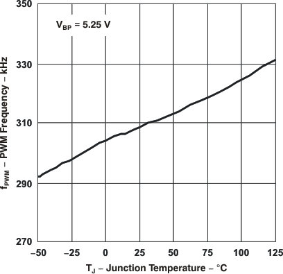
| BP | Regulator voltage | 8 V < PVDD2 < 28 V | 5 | 5.25 | 5.6 | V | |
| BPLDO | Dropout voltage | PVDD2 = 4.5 V; switching, no external load on BP | 400 | mV | |||
| IBP(1) | Regulator external load | 2 | mA | ||||
| IBPS | Regulator short circuit | 4.5 V < PVDD2 < 28 V | 10 | 20 | 30 | ||
| OSCILLATOR | |||||||
| fSW | Switching frequency | TPS54383 | 255 | 310 | 375 | kHz | |
| TPS54386 | 510 | 630 | 750 | ||||
| tDEAD(1) | Clock dead time | 140 | ns | ||||
| ERROR AMPLIFIER (EA) and VOLTAGE REFERENCE (REF) | |||||||
| VFB1 | Feedback input voltage | 0°C < TJ < +85°C | 788 | 800 | 812 | mV | |
| VFB2 | –40°C < TJ < +125°C | 786 | 812 | ||||
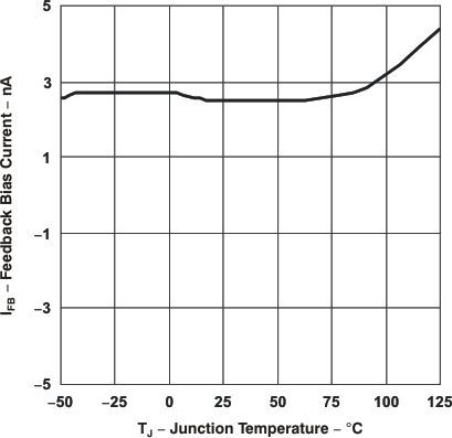
| IFB1 | Feedback input bias current | 3 | 50 | nA | |||
| IFB2 | |||||||
| gM1(1) | Transconductance | 30 | μS | ||||
| gM2(1) | |||||||
| SOFT-START (SS) | |||||||
| TSS1 | Soft-start time | 1.5 | 2.1 | 2.7 | ms | ||
| TSS2 | |||||||
| OVERCURRENT PROTECTION | |||||||
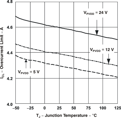
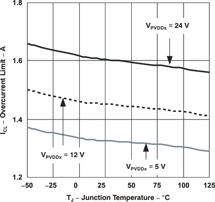
| ICL1 | Current limit channel 1 | 3.6 | 4.5 | 5.6 | A | ||
| ICL2 | Current limit channel 2 | VILIM2 = VBP | 3.6 | 4.5 | 5.6 | ||
| VILIM2 = (floating) | 2.4 | 3.0 | 3.6 | ||||
| VILIM2 = GND | 1.15 | 1.50 | 1.75 | ||||
| VUV1 | Low-level output threshold to declare a fault | Measured at feedback pin. | 670 | mV | |||
| VUV2 | |||||||
| THICCUP(1) | Hiccup timeout | 10 | ms | ||||
| tON1(oc)(1) | Minimum overcurrent pulse width | 90 | 150 | ns | |||
| tON2(oc)(1) | |||||||
| BOOTSTRAP | |||||||
| RBOOT1 | Bootstrap switch resistance | From BP to BOOT1 or BP to BOOT2, IEXT = 50 mA |
18 | Ω | |||
| RBOOT2 | |||||||
| OUTPUT STAGE (Channel 1 and Channel 2) | |||||||
| RDS(on)(1) | MOSFET on resistance plus bond wire resistance | TJ = +25°C, VPVDD2 = 8 V | 85 | mΩ | |||
| –40°C < TJ < +125°C, VPVDD2 = 8 V | 85 | 165 | |||||
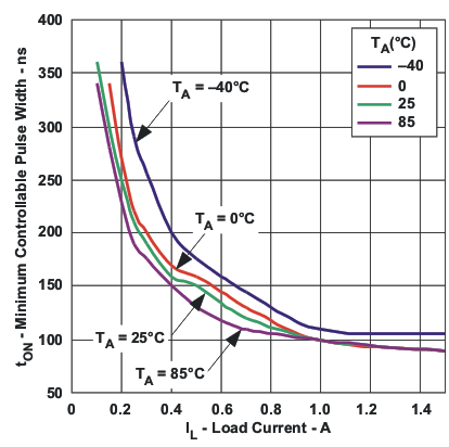
| tON(min)(1) | Minimum controllable pulse width | ISWx peak current > 1 A(3) | 100 | 200 | ns | ||
| DMIN | Minimum Duty Cycle | VFB = 0.9 V | 0 | % | |||
| DMAX | Maximum Duty Cycle | TPS54383 | fSW = 300 kHz | 90 | 95 | % | |
| TPS54386 | fSW = 600 kHz | 85 | 90 | % | |||
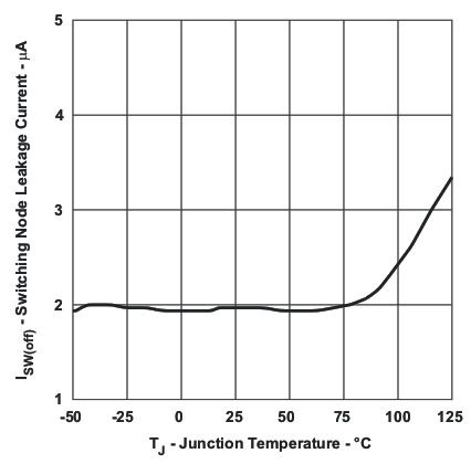
| ISW | Switching node leakage current (sourcing) | Outputs OFF | 2 | 12 | μA | ||
| THERMAL SHUTDOWN | |||||||
| TSD(1) | Shutdown temperature | 148 | °C | ||||
| TSD(hys)(1) | Hysteresis | 20 | |||||
(1) Ensured by design. Not production tested.
(2) When both outputs are started simultaneously, a 20-mA current source charges the BP capacitor. Faster times are possible with a lower BP capacitor value. More information can be found in the Input UVLO and Startup section.
(3) See Figure 14 for ISWx peak current <1 A.
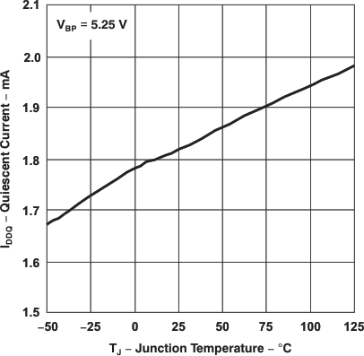
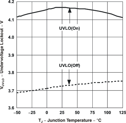
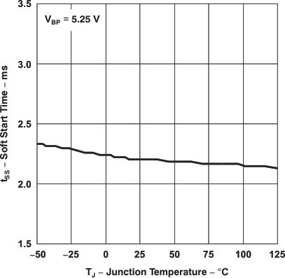
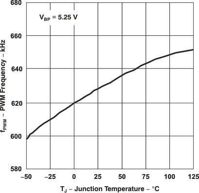
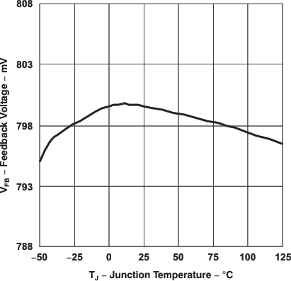
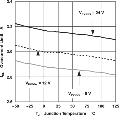
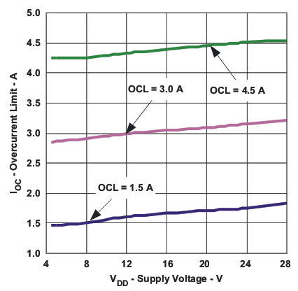
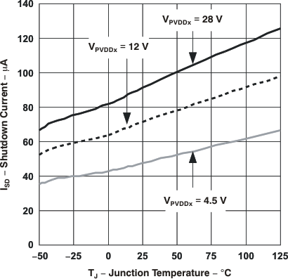
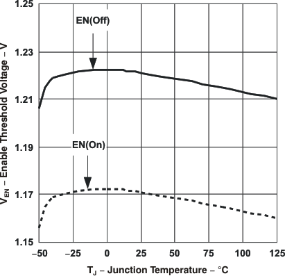
6.6 Typical Characteristics