SLVSFQ0A October 2020 – June 2021 TPS54J061
PRODUCTION DATA
- 1 Features
- 2 Applications
- 3 Description
- 4 Revision History
- 5 Pin Configuration and Functions
- 6 Specifications
-
7 Detailed Description
- 7.1 Overview
- 7.2 Functional Block Diagram
- 7.3
Feature Description
- 7.3.1 Enable and Internal LDO
- 7.3.2 Split Rail and External LDO
- 7.3.3 Output Voltage Setting
- 7.3.4 Soft Start and Output-Voltage Tracking
- 7.3.5 Frequency and Operation Mode Selection
- 7.3.6 D-CAP3 Control
- 7.3.7 Current Sense and Positive Overcurrent Protection
- 7.3.8 Low-side FET Negative Current Limit
- 7.3.9 Power Good
- 7.3.10 Overvoltage and Undervoltage Protection
- 7.3.11 Out-Of-Bounds Operation (OOB)
- 7.3.12 Output Voltage Discharge
- 7.3.13 UVLO Protection
- 7.3.14 Thermal Shutdown
- 7.4 Device Functional Modes
-
8 Application and Implementation
- 8.1 Application Information
- 8.2
Typical Application
- 8.2.1 Design Requirements
- 8.2.2
Detailed Design Procedure
- 8.2.2.1 Choose the Switching Frequency and Operation Mode (MODE Pin)
- 8.2.2.2 Choose the Output Inductor (L)
- 8.2.2.3 Set the Current Limit (TRIP)
- 8.2.2.4 Choose the Output Capacitors (COUT)
- 8.2.2.5 Choose the Input Capacitors (CIN)
- 8.2.2.6 Feedback Network (FB Pin)
- 8.2.2.7 Soft Start Capacitor (SS/REFIN Pin)
- 8.2.2.8 EN Pin Resistor Divider
- 8.2.2.9 VCC Bypass Capacitor
- 8.2.2.10 BOOT Capacitor
- 8.2.2.11 Series BOOT Resistor and RC Snubber
- 8.2.2.12 PGOOD Pullup Resistor
- 8.2.3 Application Curves
- 9 Power Supply Recommendations
- 10Layout
- 11Device and Documentation Support
- 12Mechanical, Packaging, and Ordering Information
Package Options
Mechanical Data (Package|Pins)
- RPG|14
Thermal pad, mechanical data (Package|Pins)
Orderable Information
7.3.7 Current Sense and Positive Overcurrent Protection
For a buck converter, during the on-time of the high-side FET, the switch current increases at a linear rate determined by input voltage, output voltage, and the output inductor value. During the on-time of the low-side FET, this current decreases at a linear rate determined by the output voltage and the output inductor value. The average value of the inductor current equals to the load current, IOUT.
The output overcurrent limit (OCL) in the TPS54J061 is implemented using a cycle-by-cycle valley current detect control circuit. The inductor current is monitored during the OFF state by measuring the low-side FET drain-to-source current. If the measured drain-to-source current of the low-side FET is above the current limit, the low-side FET stays ON until the current level becomes lower than the OCL level. This type of behavior reduces the average output current sourced by the device. During an overcurrent condition, the current to the load exceeds the current to the output capacitors and the output voltage tends to decrease. Eventually, when the output voltage falls below the undervoltage-protection threshold (80%), the UVP comparator shuts down the device after a wait time of 64 µs. The device will latch in the OFF state (both high-side and low-side FETs are latched off) and then restart after an approximate 14-ms delay. If the fault condition persists, the sensing detection, shut down and restart cycle repeats until the fault condition is removed.
If an OCL condition happens during start-up, then the device completes the charging of the soft-start capacitor, then trips UV when soft start is complete. Delay and attempted restart function follows as above.
The resistor, RTRIP connected from the TRIP pin to AGND sets the valley current limit threshold. Equation 4 calculates the RTRIP for a given current limit threshold.
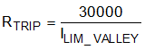
where
- ILIM_VALLEY is the valley current limit threshold in A
- RTRIP is TRIP resistor value in Ω
If an RTRIP value less than 3.74 kΩ is used, the TPS54J061 will default to an internally determined current limit clamp value.