SLVSD46A November 2017 – December 2021 TPS55160-Q1 , TPS55162-Q1 , TPS55165-Q1
PRODUCTION DATA
- 1 Features
- 2 Applications
- 3 Description
- 4 Revision History
- 5 Description (continued)
- 6 Pin Configuration and Functions
-
7 Specifications
- 7.1 Absolute Maximum Ratings
- 7.2 ESD Ratings
- 7.3 Recommended Operating Conditions
- 7.4 Thermal Information
- 7.5 Electrical Characteristics — External Components
- 7.6 Electrical Characteristics — Supply Voltage (VINP, VINL pins)
- 7.7 Electrical Characteristics — Reference Voltage (VOS_FB Pin) and Output Voltage (VOUT Pin)
- 7.8 Electrical Characteristics — Buck-Boost
- 7.9 Electrical Characteristics — Undervoltage and Overvoltage Lockout
- 7.10 Electrical Characteristics — IGN Wakeup
- 7.11 Electrical Characteristics — Logic Pins PS, IGN_PWRL, SS_EN
- 7.12 Electrical Characteristics – Overtemperature Protection
- 7.13 Electrical Characteristics – Power Good
- 7.14 Switching Characteristics — Reference Voltage (VOS_FB Pin) and Output Voltage (VOUT Pin)
- 7.15 Switching Characteristics — Buck-Boost
- 7.16 Switching Characteristics — Undervoltage and Overvoltage Lockout
- 7.17 Switching Characteristics — IGN Wakeup
- 7.18 Switching Characteristics — Logic Pins PS, IGN_PWRL, SS_EN
- 7.19 Switching Characteristics – Power Good
- 7.20 Typical Characteristics
- 8 Detailed Description
- 9 Application and Implementation
- 10Power Supply Recommendations
- 11Layout
- 12Device and Documentation Support
- 13Mechanical, Packaging, and Orderable Information
Package Options
Mechanical Data (Package|Pins)
- PWP|20
Thermal pad, mechanical data (Package|Pins)
- PWP|20
Orderable Information
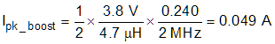
9.2.2.1.2 Inductor Current in Step-Up Mode
Use Equation 8 to calculate the inductor peak-ripple current in the step-up, or boost, mode (Ipk_boost).
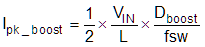
where
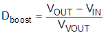
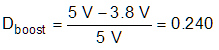
- Dboost is the duty cycle in boost mode (refer to Equation 9).
In general, the maximum peak-ripple current occurs at 50% duty cycle. In this example, because of the power derating versus the input voltage, a few calculations can find that the maximum RMS current occurs when the input voltage is approximately 3.8 V, of which the load current is 0.8 A, according to Table 9-1. Equation 10 and Equation 11 show the peak-ripple current under this condition.
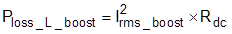
The power dissipations can be determined by the RMS current of the inductor. Use Equation 12 to calculate the RMS current of the inductor in buck mode (Irms_boost).
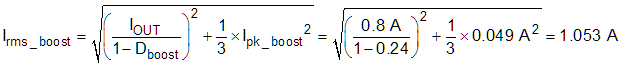
Use Equation 13 to calculate the approximate power dissipation of the inductor in boost-mode (Ploss_L_boost).