SLUSAH4D MARCH   2011  – February 2016 TPS56121

PRODUCTION DATA.  

  1. Features
  2. Applications
  3. Description
  4. Revision History
  5. Pin Configuration and Functions
  6. Specifications
    1. 6.1 Absolute Maximum Ratings
    2. 6.2 ESD Ratings
    3. 6.3 Recommended Operating Conditions
    4. 6.4 Thermal Information
    5. 6.5 Electrical Characteristics
    6. 6.6 Typical Characteristics
  7. Detailed Description
    1. 7.1 Overview
    2. 7.2 Functional Block Diagram
    3. 7.3 Feature Description
      1. 7.3.1  Voltage Reference
      2. 7.3.2  Enable Functionality, Startup Sequence and Timing
        1. 7.3.2.1 COMP Pin Impedance Sensing
        2. 7.3.2.2 Overcurrent Protection (OCP) Setting
      3. 7.3.3  Soft-Start Time
      4. 7.3.4  Oscillator
      5. 7.3.5  Overcurrent Protection (OCP)
      6. 7.3.6  Switching Node (SW)
      7. 7.3.7  Input Undervoltage Lockout (UVLO)
      8. 7.3.8  Pre-Bias Startup
      9. 7.3.9  Power Good
      10. 7.3.10 Thermal Shutdown
    4. 7.4 Device Functional Modes
  8. Application and Implementation
    1. 8.1 Application Information
    2. 8.2 Typical Application
      1. 8.2.1 Design Requirements
      2. 8.2.2 Detailed Design Procedure
        1. 8.2.2.1  Switching Frequency Selection
        2. 8.2.2.2  Inductor Selection (L1)
        3. 8.2.2.3  Output Capacitor Selection
        4. 8.2.2.4  Inductor Peak Current Rating
        5. 8.2.2.5  Input Capacitor Selection
        6. 8.2.2.6  Bootstrap Capacitor (C14)
        7. 8.2.2.7  Bootstrap Resistor (R2)
        8. 8.2.2.8  RC Snubber (R9 and C18)
        9. 8.2.2.9  VDD Bypass Capacitor (C11)
        10. 8.2.2.10 BP5 Bypass Capacitor (C12)
        11. 8.2.2.11 Soft-Start Capacitor (C13)
        12. 8.2.2.12 Current Limit (R1)
        13. 8.2.2.13 Feedback Divider (R4, R7)
        14. 8.2.2.14 Compensation (C15, C16, C17, R3, R6)
      3. 8.2.3 Application Curves
  9. Power Supply Recommendations
  10. 10Layout
    1. 10.1 Layout Guidelines
    2. 10.2 Layout Example
  11. 11Device and Documentation Support
    1. 11.1 Device Support
      1. 11.1.1 Third-Party Products Disclaimer
    2. 11.2 Trademarks
    3. 11.3 Electrostatic Discharge Caution
    4. 11.4 Glossary
  12. 12Mechanical, Packaging, and Orderable Information

Package Options

Mechanical Data (Package|Pins)
Thermal pad, mechanical data (Package|Pins)
Orderable Information

5 Pin Configuration and Functions

DQP PACKAGE
PQFN-22
(TOP VIEW)
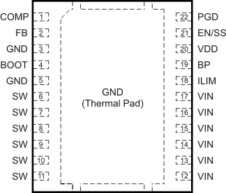
TPS56121 pinout_dqp22_lusah5.gif
Note: The thermal pad is also an electrical ground connection.

Pin Functions

PIN I/O DESCRIPTION
NAME NO.
BOOT 4 O Gate drive voltage for the high-side FET. A 100-nF capacitor (typical) must be connected between this pin and the SW pin. To reduce a voltage spike at SW, a BOOT resistor with a value between 5 Ω to 15 Ω may be placed in series with the BOOT capacitor to slow down turn-on of the high-side FET.
BP 19 O Output bypass for the internal regulator. Connect a low-ESR bypass ceramic capacitor of 1 µF or greater from this pin to GND.
COMP 1 O Output of the error amplifier and connection node for loop feedback components. Optionally, a 40.2 kΩ resistor from this pin to GND sets switching frequency to 300KHz instead of the default value of 500 kHz; while a 13.3-kΩ resistor from this pin to GND sets switching frequency to 1 MHz.
EN/SS 21 I Logic-level input starts or stops the controller via an external user command. Allowing this pin to float turns the controller on. Pulling this pin low disables the controller. This is also the soft-start programming pin. A capacitor connected from this pin to GND programs the soft-start time. The capacitor is charged with an internal current source of 10 µA. The resulting voltage ramp of this pin is also used as a second non-inverting input to the error amplifier after a 0.8 V (typical) level shift downwards. Output regulation is controlled by the internal level shifted voltage ramp until that voltage reaches the internal reference voltage of 600 mV. The voltage ramp of this pin reaches 1.4 V (typical).
FB 2 I Inverting input to the error amplifier. In normal operation, the voltage on this pin is equal to the internal reference voltage.
GND 3 Ground reference for the device
5
GND Thermal Pad Ground reference for the device. This is also the thermal pad used to conduct heat from the device. This connection serves two purposes. The first is to provide an electrical ground connection for the device. The second is to provide a low thermal impedance path from the device die to the PCB. This pad should be tied externally to a ground plane.
ILIM 18 I A resistor connected from this pin to GND sets the overcurrent threshold for the device (the low-side FET).
PGD 22 O Open drain power good output.
SW 6 I Switching node of the power conversion stage. Sense line for the adaptive anti-cross conduction circuitry. Acts as the common connection for the flying high-side FET driver.
7
8
9
10
11
VDD 20 I Power input to the controller. A low-ESR bypass ceramic capacitor of 1 µF should be connected from this pin close to GND.
VIN 12 I Power input to the high-side FET.
13
14
15
16
17