SLVSD91C December 2015 – April 2024 TPS562201 , TPS562208
PRODUCTION DATA
- 1
- 1 Features
- 2 Applications
- 3 Description
- 4 Pin Configuration and Functions
- 5 Specifications
- 6 Detailed Description
- 7 Application and Implementation
- 8 Device and Documentation Support
- 9 Revision History
- 10Mechanical, Packaging, and Orderable Information
Package Options
Mechanical Data (Package|Pins)
- DDC|6
Thermal pad, mechanical data (Package|Pins)
Orderable Information
5.6 Typical Characteristics
VIN = 12 V (unless otherwise noted)
 Figure 5-1 TPS562201 Supply Current vs Junction Temperature
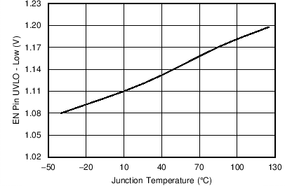 Figure 5-3 EN
Pin UVLO Low Voltage vs Junction Temperature
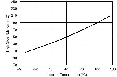 Figure 5-5 High-Side Rds-on vs Junction Temperature
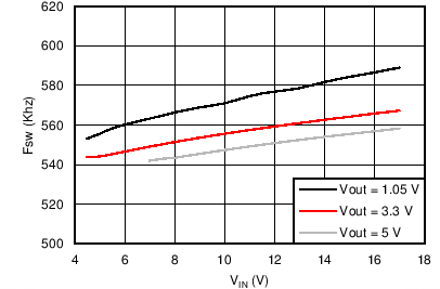
| Iout = 10 mA | ||
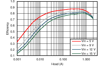 Figure 5-9 TPS562201 VOUT = 1.05 V Efficiency, L = 2.2 µH
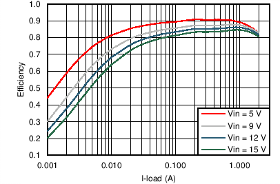 Figure 5-11 TPS562201 VOUT = 1.8 V Efficiency, L = 2.2 µH
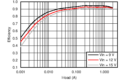 Figure 5-13 TPS562201 VOUT = 5 V Efficiency, L = 3.3 µH
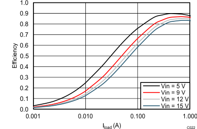 Figure 5-15 TPS562208 VOUT = 1.5 V Efficiency, L = 2.2 µH
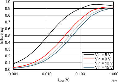 Figure 5-17 TPS562208 VOUT = 3.3 V Efficiency, L = 2.2 µH
 Figure 5-2 VFB
Voltage vs Junction Temperature
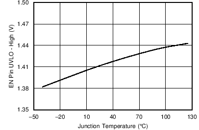 Figure 5-4 EN
Pin UVLO High Voltage vs Junction Temperature
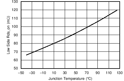 Figure 5-6 Low-Side Rds-on vs Junction Temperature
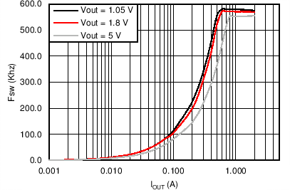
| VIN = 12 V | ||
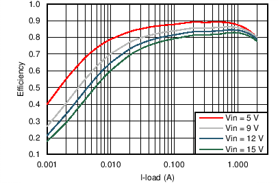 Figure 5-10 TPS562201 VOUT = 1.5 V Efficiency, L = 2.2 µH
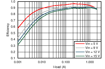 Figure 5-12 TPS562201 VOUT = 3.3 V Efficiency, L = 3.3 µH
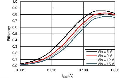 Figure 5-14 TPS562208 VOUT = 1.05 V Efficiency, L = 2.2 µH
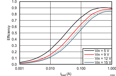 Figure 5-16 TPS562208 VOUT = 1.8 V Efficiency, L = 2.2 µH
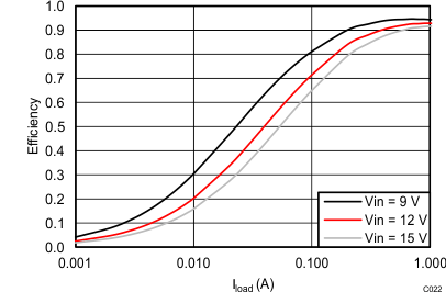 Figure 5-18 TPS562208 VOUT = 5 V Efficiency, L = 3.3 µH