SLVSCB0E january 2014 – may 2023 TPS562200 , TPS563200
PRODUCTION DATA
- 1 Features
- 2 Applications
- 3 Description
- 4 Revision History
- 5 Pin Configuration and Functions
- 6 Specifications
- 7 Detailed Description
- 8 Application and Implementation
- 9 Device and Documentation Support
- 10Mechanical, Packaging, And Orderable Information
Package Options
Mechanical Data (Package|Pins)
- DDC|6
Thermal pad, mechanical data (Package|Pins)
Orderable Information
8.2.1.2.3 Output Filter Selection
The LC filter used as the output filter has double pole at:
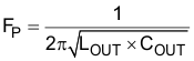
At low frequencies, the overall loop gain is set by the output set-point resistor divider network and the internal gain of the device. The low frequency phase is 180 degrees. At the output filter pole frequency, the gain rolls off at a –40 dB per decade rate and the phase drops rapidly. D-CAP2 control scheme introduces a high frequency zero that reduces the gain roll off to –20 dB per decade and increases the phase to 90 degrees one decade above the zero frequency. The inductor and capacitor selected for the output filter must be selected so that the double pole of Equation 3 is located below the high frequency zero but close enough that the phase boost provided be the high frequency zero provides adequate phase margin for a stable circuit. To meet this requirement use the values recommended in Table 1.
| Output Voltage (V) | R2 (kΩ) | R3 (kΩ) | L1(uH) | C5 + C6 (µF) | ||
|---|---|---|---|---|---|---|
| MIN | TYP | MAX | ||||
| 1 | 3.09 | 10.0 | 1.5 | 2.2 | 4.7 | 20 - 68 |
| 1.05 | 3.74 | 10.0 | 1.5 | 2.2 | 4.7 | 20 - 68 |
| 1.2 | 5.76 | 10.0 | 1.5 | 2.2 | 4.7 | 20 - 68 |
| 1.5 | 9.53 | 10.0 | 1.5 | 2.2 | 4.7 | 20 - 68 |
| 1.8 | 13.7 | 10.0 | 1.5 | 2.2 | 4.7 | 20 - 68 |
| 2.5 | 22.6 | 10.0 | 2.2 | 3.3 | 4.7 | 20 - 68 |
| 3.3 | 33.2 | 10.0 | 2.2 | 3.3 | 4.7 | 20 - 68 |
| 5 | 54.9 | 10.0 | 3.3 | 4.7 | 4.7 | 20 - 68 |
| 6.5 | 75 | 10.0 | 3.3 | 4.7 | 4.7 | 20 - 68 |
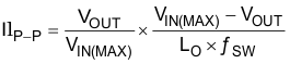
The inductor peak-to-peak ripple current, peak current and RMS current are calculated using Equation 4, Equation 5 and Equation 6. The inductor saturation current rating must be greater than the calculated peak current and the RMS or heating current rating must be greater than the calculated RMS current. Use 650 kHz for ƒSW.
Use 650 kHz for ƒSW. Make sure the chosen inductor is rated for the peak current of Equation 5 and the RMS current of Equation 6.
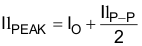
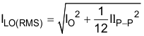
For this design example, the calculated peak current is 2.34 A and the calculated RMS current is 2.01 A. The inductor used is a TDK CLF7045T-2R2N with a peak current rating of 5.5 A and an RMS current rating of 4.3 A
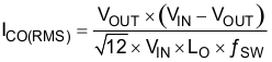
The capacitor value and ESR determines the amount of output voltage ripple. The device is intended for use with ceramic or other low ESR capacitors. Recommended values range from 20 µF to 68 µF. Use Equation 7 to determine the required RMS current rating for the output capacitor.
For this design, two TDK C3216X5R0J226M 22-µF output capacitors are used. The typical ESR is 2 mΩ each. The calculated RMS current is 0.286 A and each output capacitor is rated for 4 A.