SLVSA02B September 2009 – January 2019 TPS60151
PRODUCTION DATA.
- 1 Features
- 2 Applications
- 3 Description
- 4 Revision History
- 5 Device Comparison Table
- 6 Pin Configuration and Functions
- 7 Specifications
- 8 Detailed Description
- 9 Application and Implementation
- 10Power Supply Recommendations
- 11Layout
- 12Device and Documentation Support
- 13Mechanical, Packaging, and Orderable Information
Package Options
Mechanical Data (Package|Pins)
- DRV|6
Thermal pad, mechanical data (Package|Pins)
- DRV|6
Orderable Information
9.2.2.1 Capacitor Selection
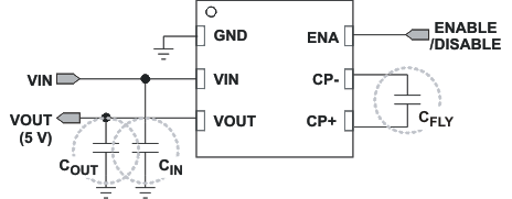
For minimum output voltage ripple, the output capacitor (COUT) should be a surface-mount ceramic capacitor. Tantalum capacitors generally have a higher effective series resistance (ESR) and may contribute to higher output voltage ripple. Leaded capacitors also increase ripple due to the higher inductance of the package itself. To achieve the best operation with low input voltage and high load current, the input and flying capacitors (CIN and CFLY, respectively) should also be surface-mount ceramic types.
 Figure 11. Capacitors
 Generally, CFLY can be calculated by the following simple equation,

Both equation should be same, 

If ILOAD = 140 mA, f = 1.5 MHz, and ΔVCFLY = 100 mV, the minimum value of the flying capacitor should be 1 μF.
Output capacitance, COUT, is also strongly related to output ripple voltage and loop stability,

The minimum output capacitance for all output levels is 2.2 μF due to control stability. Larger ceramic capacitors or low ESR capacitors can be used to lower the output ripple voltage.
Table 1. Suggested Capacitors (Input / Output / Flying Capacitor)
| VALUE | DIELECTRIC MATERIAL | PACKAGE SIZE | RATED VOLTAGE |
|---|---|---|---|
| 4.7 μF | X5R or X7R | 0603 | 10 V |
| 2.2 μF | X5R or X7R | 0603 | 10 V |
The efficiency of the charge pump regulator varies with the output voltage, the applied input voltage and the load current.
The approximate efficiency in normal operating mode is given by:

