SLVS324C July 2001 – October 2020 TPS60400 , TPS60401 , TPS60402 , TPS60403
PRODUCTION DATA
- 1 Features
- 2 Applications
- 3 Description
- 4 Revision History
- 5 Device Comparison Table
- 6 Pin Configuration and Functions
- 7 Specifications
- 8 Detailed Description
- 9 Application and Implementation
- 10Power Supply Recommendations
- 11Layout
- 12Device and Documentation Support
- 13Mechanical, Packaging, and Orderable Information
Package Options
Refer to the PDF data sheet for device specific package drawings
Mechanical Data (Package|Pins)
- DBV|5
Thermal pad, mechanical data (Package|Pins)
Orderable Information
6 Pin Configuration and Functions
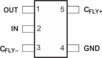
 Figure 6-1 DBV Package5 PinsTop View
Table 6-1 Pin Functions
| PIN | I/O | DESCRIPTION | |
|---|---|---|---|
| NAME | NO. | ||
| CFLY+ | 5 | Positive terminal of the flying capacitor C(fly) | |
| CFLY- | 3 | Negative terminal of the flying capacitor C(fly) | |
| GND | 4 | Ground | |
| IN | 2 | I | Supply input. Connect to an input supply in the 1.6-V to 5.5-V range. Bypass IN to GND with a capacitor that has the same value as the flying capacitor. |
| OUT | 1 | O | Power output with VO = -VI Bypass OUT to GND with the output filter capacitor CO. |