SLVS314F SEPTEMBER 2000 – August 2015 TPS61010 , TPS61012 , TPS61013 , TPS61014 , TPS61015 , TPS61016
PRODUCTION DATA.
- 1 Features
- 2 Applications
- 3 Description
- 4 Revision History
- 5 Device Comparison Table
- 6 Pin Configuration and Functions
- 7 Specifications
- 8 Parameter Measurement Information
- 9 Detailed Description
-
10Application and Implementation
- 10.1 Application Information
- 10.2
Typical Applications
- 10.2.1 1.8-mm Maximum Height Power Supply With Single Battery Cell Input Using Low Profile Components
- 10.2.2 250-mA Power Supply With Two Battery Cell Input
- 10.2.3 Dual Output Voltage Power Supply for DSPs
- 10.2.4 Power Supply With Auxiliary Positive Output Voltage
- 10.2.5 Power Supply With Auxiliary Negative Output Voltage
- 10.2.6 TPS6101x EVM Circuit Diagram
- 11Power Supply Recommendations
- 12Layout
- 13Device and Documentation Support
- 14Mechanical, Packaging, and Orderable Information
Package Options
Refer to the PDF data sheet for device specific package drawings
Mechanical Data (Package|Pins)
- DGS|10
Thermal pad, mechanical data (Package|Pins)
Orderable Information
10 Application and Implementation
NOTE
Information in the following applications sections is not part of the TI component specification, and TI does not warrant its accuracy or completeness. TI’s customers are responsible for determining suitability of components for their purposes. Customers should validate and test their design implementation to confirm system functionality.
10.1 Application Information
The devices are designed to operate from an input voltage supply range between 0.9 V and 3.3 V with a maximum switch current limit up to 1300mA. The devices operate in PWM mode from the medium to heavy load conditions and in power save mode at light load condition. In PWM mode the TPS6101x converter operates with the nominal switching frequency of 500kHz. As the load current decreases, the converter enters power save mode, reducing the switching frequency and minimizing the IC quiescent current to achieve high efficiency over the entire load current range.
10.2 Typical Applications
10.2.1 1.8-mm Maximum Height Power Supply With Single Battery Cell Input Using Low Profile Components
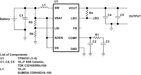 Figure 19. 1.8-mm Maximum Height Power Supply With Single Battery Cell Input Using Low Profile Components Schematic
10.2.1.1 Design Requirements
Use the following typical application design procedure to select external components values for the TPS6101x device.
Table 2. TPS61010 3.3 V Output Design Parameters
| DESIGN PARAMETERS | EXAMPLE VALUES |
|---|---|
| Input Voltage Range | 0.9 V to 3.3 V |
| Output Voltage | 3.3 V |
| Output Voltage Ripple | ±3% VOUT |
| Transient Response | ±10% VOUT |
| Input Voltage Ripple | ±200 mV |
| Output Current Rating | 200 mA |
| Operating Frequency | 500 kHz |
10.2.1.2 Detailed Design Procedure
The TPS6101x boost converter family is intended for systems that are powered by a single-cell NiCd or NiMH battery with a typical terminal voltage between 0.9 V to 1.6 V. It can also be used in systems that are powered by two-cell NiCd or NiMH batteries with a typical stack voltage between 1.8 V and 3.2 V. Additionally, single- or dual-cell, primary and secondary alkaline battery cells can be the power source in systems where the TPS6101x is used.
10.2.1.2.1 Programming the TPS61010 Adjustable Output Voltage Device
The output voltage of the TPS61010 can be adjusted with an external resistor divider. The typical value of the voltage on the FB pin is 500 mV in fixed frequency operation and 485 mV in the power-save operation mode. The maximum allowed value for the output voltage is 3.3 V. The current through the resistive divider should be about 100 times greater than the current into the FB pin. The typical current into the FB pin is 0.01 µA, and the voltage across R4 is typically 500 mV. Based on those two values, the recommended value for R4 is in the range of 500 kΩ in order to set the divider current at 1 µA. From that, the value of resistor R3, depending on the needed output voltage (VO), can be calculated using Equation 1.

If, as an example, an output voltage of 2.5 V is needed, a 2-MΩ resistor should be chosen for R3.
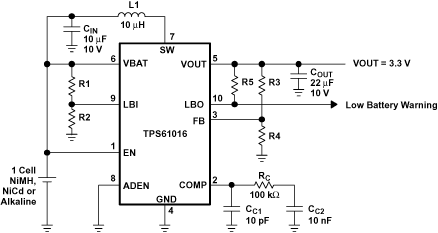 Figure 20. Typical Application Circuit for Adjustable Output Voltage Option
The output voltage of the adjustable output voltage version changes with the output current. Due to device-internal ground shift, which is caused by the high switch current, the internal reference voltage and the voltage on the FB pin increases with increasing output current. Since the output voltage follows the voltage on the FB pin, the output voltage rises as well with a rate of 1 mV per 1-mA output current increase. Additionally, when the converter goes into pulse-skip mode at output currents around 5 mA and lower, the output voltage drops due to the hysteresis of the controller. This hysteresis is about 15 mV, measured on the FB pin.
10.2.1.2.2 Programming the Low Battery Comparator Threshold Voltage
The current through the resistive divider should be about 100 times greater than the current into the LBI pin. The typical current into the LBI pin is 0.01 µA, the voltage across R2 is equal to the reference voltage that is generated on-chip, which has a value of 500 mV ±15 mV. The recommended value for R2 is therefore in the range of 500 kΩ. From that, the value of resistor R1, depending on the desired minimum battery voltage VBAT, can be calculated using Equation 2.

For example, if the low-battery detection circuit should flag an error condition on the LBO output pin at a battery voltage of 1 V, a resistor in the range of 500 kΩ should be chosen for R1. The output of the low battery comparator is a simple open-drain output that goes active low if the battery voltage drops below the programmed threshold voltage on LBI. The output requires a pullup resistor with a recommended value of 1 MΩ, and should only be pulled up to the VO. If not used, the LBO pin can be left floating or tied to GND.
10.2.1.2.3 Inductor Selection
A boost converter normally requires two main passive components for storing energy during the conversion. A boost inductor is required and a storage capacitor at the output. To select the boost inductor, it is recommended to keep the possible peak inductor current below the current limit threshold of the power switch in the chosen configuration. For example, the current limit threshold of the TPS61010's switch is 1100 mA at an output voltage of 3.3 V. The highest peak current through the inductor and the switch depends on the output load, the input (VBAT), and the output voltage (VO). Estimation of the maximum average inductor current can be done using Equation 3.

For example, for an output current of 100 mA at 3.3 V, at least 515-mA of current flows through the inductor at a minimum input voltage of 0.8 V.
The second parameter for choosing the inductor is the desired current ripple in the inductor. Normally, it is advisable to work with a ripple of less than 20% of the average inductor current. A smaller ripple reduces the magnetic hysteresis losses in the inductor, as well as output voltage ripple and EMI. But in the same way, regulation time at load changes rises. In addition, a larger inductor increases the total system costs.
With those parameters, it is possible to calculate the value for the inductor by using Equation 4.

Parameter 7 is the switching frequency and Δ IL is the ripple current in the inductor, that is, 20% × IL.
In this example, the desired inductor has the value of 12 µH. With this calculated value and the calculated currents, it is possible to choose a suitable inductor. Care must be taken that load transients and losses in the circuit can lead to higher currents as estimated in Equation 3. Also, the losses in the inductor caused by magnetic hysteresis losses and copper losses are a major parameter for total circuit efficiency.
The following inductor series from different suppliers were tested. All work with the TPS6101x converter within their specified parameters:
Table 3. Recommended Inductors
| VENDOR | RECOMMENDED INDUCTOR SERIES |
|---|---|
| Sumida | Sumida CDR74B |
| Sumida CDRH74 | |
| Sumida CDRH5D18 | |
| Sumida CDRH6D38 | |
| Coilcraft | Coilcraft DO 1608C |
| Coilcraft DS 1608C | |
| Coilcraft DS 3316 | |
| Coilcraft DT D03308P | |
| Coiltronics | Coiltronics UP1B |
| Coiltronics UP2B | |
| Murata | Murata LQS66C |
| Murata LQN6C | |
| TDK | TDK SLF 7045 |
| TDK SLF 7032 |
10.2.1.2.4 Capacitor Selection
The major parameter necessary to define the output capacitor is the maximum allowed output voltage ripple of the converter. This ripple is determined by two parameters of the capacitor, the capacitance and the ESR. It is possible to calculate the minimum capacitance needed for the defined ripple, supposing that the ESR is zero, by using Equation 5.

Parameter f is the switching frequency and ΔV is the maximum allowed ripple.
With a chosen ripple voltage of 15 mV, a minimum capacitance of 10 µF is needed. The total ripple is larger due to the ESR of the output capacitor. This additional component of the ripple can be calculated using Equation 6.

An additional ripple of 30 mV is the result of using a tantalum capacitor with a low ESR of 300 mΩ. The total ripple is the sum of the ripple caused by the capacitance and the ripple caused by the ESR of the capacitor. In this example, the total ripple is 45 mV. It is possible to improve the design by enlarging the capacitor or using smaller capacitors in parallel to reduce the ESR or by using better capacitors with lower ESR, like ceramics. For example, a 10 µF ceramic capacitor with an ESR of 50 mΩ is used on the evaluation module (EVM). Tradeoffs must be made between performance and costs of the converter circuit.
A 10-µF input capacitor is recommended to improve transient behavior of the regulator. A ceramic capacitor or a tantalum capacitor with a 100 nF ceramic capacitor in parallel placed close to the IC is recommended.
10.2.1.2.5 Compensation of the Control Loop
An R/C/C network must be connected to the COMP pin in order to stabilize the control loop of the converter. Both the pole generated by the inductor L1 and the zero caused by the ESR and capacitance of the output capacitor must be compensated. The network shown in Figure 21 satisfies these requirements.
 Figure 21. Compensation of Control Loop
Resistor RC and capacitor CC2 depend on the chosen inductance. For a 10 µH inductor, the capacitance of CC2 should be chosen to 10 nF, or in other words, if the inductor is XX µH, the chosen compensation capacitor should be XX nF, the same number value. The value of the compensation resistor is then chosen based on the requirement to have a time constant of 1 ms, for the R/C network RC and CC2, hence for a 33 nF capacitor, a 33 kΩ resistor should be chosen for RC.
Capacitor CC1 depends on the ESR and capacitance value of the output capacitor, and on the value chosen for RC. Its value is calculated using Equation 7.

For a selected output capacitor of 22 µF with an ESR of 0.2Ω , an RC of 33 kΩ, the value of CC1 is in the range of 100 pF.
Table 4. Recommended Compensation Components
| INDUCTOR [µH] | OUTPUT CAPACITOR | RC [kΩ] | CC1 [pF] | CC2 [nF] | |
|---|---|---|---|---|---|
| CAPACITANCE [µF] | ESR [Ω] | ||||
| 33 | 22 | 0.2 | 33 | 120 | 33 |
| 22 | 22 | 0.3 | 47 | 150 | 22 |
| 10 | 22 | 0.4 | 100 | 100 | 10 |
| 10 | 10 | 0.1 | 100 | 10 | 10 |
10.2.1.3 Application Curves
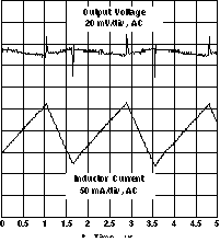 Figure 22. Output Voltage Ripple in Continuous Mode
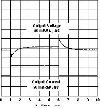 Figure 24. Load Transient Response
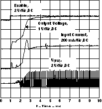 Figure 26. Converter Start-Up Time After Enable
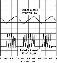 Figure 23. Output Voltage Ripple in Discontinuous Mode
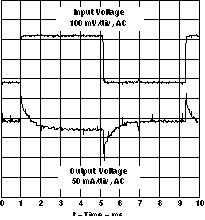 Figure 25. Line Transient Response
10.2.2 250-mA Power Supply With Two Battery Cell Input
TPS6101x application schematic of 2 Cell AA Battery Input and >250-mA output current.
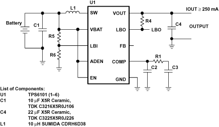 Figure 27. 250-mA Power Supply With Two Battery Cell Input
10.2.3 Dual Output Voltage Power Supply for DSPs
TPS6101x application schematic with 3.3Vout of I/O supply and post LDO 1.5Vout of DSP core supply.
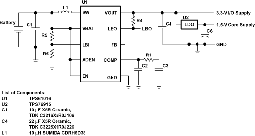 Figure 28. Dual Output Voltage Power Supply for DSPs
10.2.4 Power Supply With Auxiliary Positive Output Voltage
TPS6101x application schematic of 3.3Vout and 6Vout with charge pump.
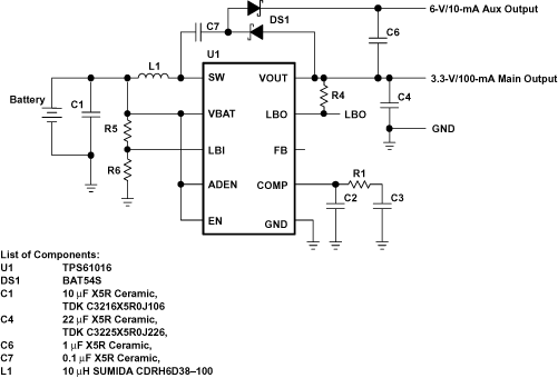 Figure 29. Power Supply With Auxiliary Positive Output Voltage
10.2.5 Power Supply With Auxiliary Negative Output Voltage
TPS6101x application schematic of 3.3Vout and -2.7Vout with charge pump.
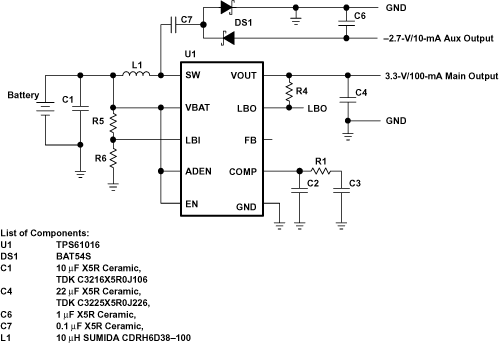 Figure 30. Power Supply With Auxiliary Negative Output Voltage
10.2.6 TPS6101x EVM Circuit Diagram
TPS6101x application schematic of the standard EVM configuration.
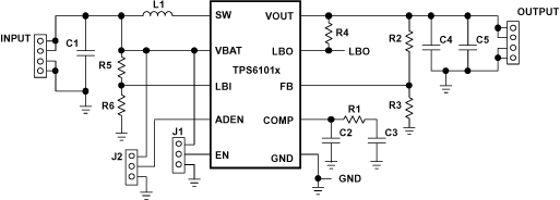 Figure 31. TPS6101x EVM Circuit Diagram