SLVS314F SEPTEMBER   2000  – August 2015 TPS61010 , TPS61012 , TPS61013 , TPS61014 , TPS61015 , TPS61016

PRODUCTION DATA.  

  1. Features
  2. Applications
  3. Description
  4. Revision History
  5. Device Comparison Table
  6. Pin Configuration and Functions
  7. Specifications
    1. 7.1 Absolute Maximum Ratings
    2. 7.2 ESD Ratings
    3. 7.3 Recommended Operating Conditions
    4. 7.4 Thermal Information
    5. 7.5 Electrical Characteristics
    6. 7.6 Typical Characteristics
      1. 7.6.1 Table of Graphs
  8. Parameter Measurement Information
  9. Detailed Description
    1. 9.1 Overview
    2. 9.2 Functional Block Diagram
    3. 9.3 Feature Description
      1. 9.3.1 Controller Circuit
      2. 9.3.2 Synchronous Rectifier
      3. 9.3.3 Power-Save Mode
      4. 9.3.4 Device Enable
      5. 9.3.5 Undervoltage Lockout (UVLO)
      6. 9.3.6 Autodischarge
      7. 9.3.7 Low-Battery Detector Circuit (LBI and LBO)
      8. 9.3.8 Antiringing Switch
      9. 9.3.9 Adjustable Output Voltage
    4. 9.4 Device Functional Modes
  10. 10Application and Implementation
    1. 10.1 Application Information
    2. 10.2 Typical Applications
      1. 10.2.1 1.8-mm Maximum Height Power Supply With Single Battery Cell Input Using Low Profile Components
        1. 10.2.1.1 Design Requirements
        2. 10.2.1.2 Detailed Design Procedure
          1. 10.2.1.2.1 Programming the TPS61010 Adjustable Output Voltage Device
          2. 10.2.1.2.2 Programming the Low Battery Comparator Threshold Voltage
          3. 10.2.1.2.3 Inductor Selection
          4. 10.2.1.2.4 Capacitor Selection
          5. 10.2.1.2.5 Compensation of the Control Loop
        3. 10.2.1.3 Application Curves
      2. 10.2.2 250-mA Power Supply With Two Battery Cell Input
      3. 10.2.3 Dual Output Voltage Power Supply for DSPs
      4. 10.2.4 Power Supply With Auxiliary Positive Output Voltage
      5. 10.2.5 Power Supply With Auxiliary Negative Output Voltage
      6. 10.2.6 TPS6101x EVM Circuit Diagram
  11. 11Power Supply Recommendations
  12. 12Layout
    1. 12.1 Layout Guidelines
    2. 12.2 Layout Example
    3. 12.3 Thermal Considerations
  13. 13Device and Documentation Support
    1. 13.1 Device Support
      1. 13.1.1 Third-Party Products Disclaimer
    2. 13.2 Related Links
    3. 13.3 Community Resources
    4. 13.4 Trademarks
    5. 13.5 Electrostatic Discharge Caution
    6. 13.6 Glossary
  14. 14Mechanical, Packaging, and Orderable Information

Package Options

Refer to the PDF data sheet for device specific package drawings

Mechanical Data (Package|Pins)
  • DGS|10
Thermal pad, mechanical data (Package|Pins)
Orderable Information

8 Parameter Measurement Information
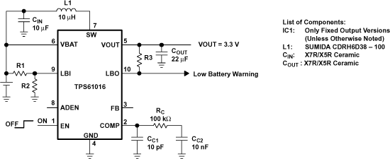
TPS61010 TPS61011 TPS61012 TPS61013 TPS61014 TPS61015 TPS61016 pmi_charmea_LVS314.gifFigure 16. Circuit Used for Typical Characteristics Measurements