SLVSDX7D January 2019 – July 2021 TPS61022
PRODUCTION DATA
- 1 Features
- 2 Applications
- 3 Description
- 4 Revision History
- 5 Pin Configuration and Functions
- 6 Specifications
- 7 Detailed Description
- 8 Application and Implementation
- 9 Power Supply Recommendations
- 10Layout
- 11Device and Documentation Support
- 12Mechanical, Packaging, and Orderable Information
Package Options
Mechanical Data (Package|Pins)
- RWU|7
Thermal pad, mechanical data (Package|Pins)
Orderable Information
7.4.2 Power-Save Mode
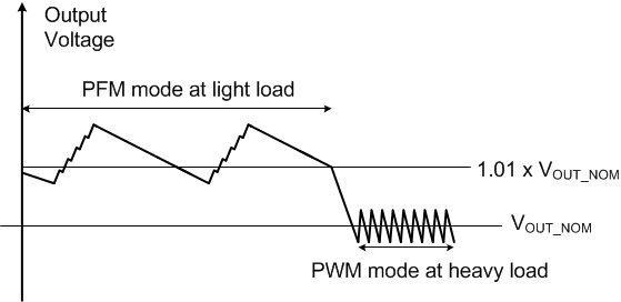
The TPS61022 integrates a power-save mode with PFM to improve efficiency at light load. When the load current decreases, the inductor valley current set by the output of the error amplifier no longer regulates the output voltage. When the inductor valley current hits the low limit of 150 mA, the output voltage exceeds the setting voltage as the load current decreases further. When the FB voltage hits the PFM reference voltage, the TPS61022 goes into the power-save mode. In the power-save mode, when the FB voltage rises and hits the PFM reference voltage, the device continues switching for several cycles because of the delay time of the internal comparator — then it stops switching. The load is supplied by the output capacitor, and the output voltage declines. When the FB voltage falls below the PFM reference voltage, after the delay time of the comparator, the device starts switching again to ramp up the output voltage.
 Figure 7-1 Output Voltage in PWM
Mode and PFM Mode