SLVS413K October 2002 – July 2022 TPS61040 , TPS61041
PRODUCTION DATA
- 1 Features
- 2 Applications
- 3 Description
- 4 Revision History
- 5 Pin Configuration and Functions
- 6 Specifications
- 7 Detailed Description
- 8 Application and Implementation
- 9 Power Supply Recommendations
- 10Layout
- 11Device and Documentation Support
- 12Mechanical, Packaging, and Orderable Information
Package Options
Refer to the PDF data sheet for device specific package drawings
Mechanical Data (Package|Pins)
- DBV|5
- DDC|5
- DRV|6
Thermal pad, mechanical data (Package|Pins)
- DRV|6
Orderable Information
8.2.2.1 Inductor Selection, Maximum Load Current
Because the PFM peak current control scheme is inherently stable, the inductor value does not affect the stability of the regulator. The selection of the inductor together with the nominal load current, input and output voltage of the application determines the switching frequency of the converter. Depending on the application, inductor values from 2.2 μH to 47 μH are recommended. The maximum inductor value is determined by the maximum on time of the switch, typically 6 μs. The peak current limit of 400 mA/250 mA (typically) should be reached within this 6-μs period for proper operation.
The inductor value determines the maximum switching frequency of the converter. Therefore, select the inductor value that ensures the maximum switching frequency at the converter maximum load current is not exceeded. The maximum switching frequency is calculated by the following formula:
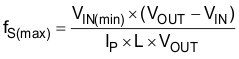
where
- IP = Peak current as described in Peak Current Control
- L = Selected inductor value
- VIN(min) = The highest switching frequency occurs at the minimum input voltage
If the selected inductor value does not exceed the maximum switching frequency of the converter, the next step is to calculate the switching frequency at the nominal load current using the following formula:
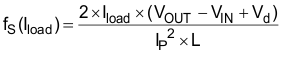
where
- IP = Peak current as described in Peak Current Control
- L = Selected inductor value
- Iload = Nominal load current
- Vd = Rectifier diode forward voltage (typically 0.3 V)
A smaller inductor value gives a higher converter switching frequency, but lowers the efficiency.
The inductor value has less effect on the maximum available load current and is only of secondary order. The best way to calculate the maximum available load current under certain operating conditions is to estimate the expected converter efficiency at the maximum load current. This number can be taken out of the efficiency graphs shown in Figure 6-1 through Figure 6-4. The maximum load current can then be estimated as follows:
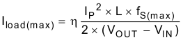
where
- IP = Peak current as described in Peak Current Control
- L = Selected inductor value
- fSmax = Maximum switching frequency as calculated previously
- η = Expected converter efficiency. Typically 70% to 85%
The maximum load current of the converter is the current at the operation point where the converter starts to enter the continuous conduction mode. Usually the converter should always operate in discontinuous conduction mode.
Last, the selected inductor should have a saturation current that meets the maximum peak current of the converter (as calculated in Peak Current Control). Use the maximum value for ILIM for this calculation.
Another important inductor parameter is the dc resistance. The lower the dc resistance, the higher the efficiency of the converter. See Table 8-2 and the typical applications for the inductor selection.
| DEVICE | INDUCTOR VALUE | COMPONENT SUPPLIER(1) | COMMENTS |
|---|---|---|---|
| TPS61040 | 10 μH | Sumida CR32-100 | High efficiency |
| 10 μH | Sumida CDRH3D16-100 | High efficiency | |
| 10 μH | Murata LQH4C100K04 | High efficiency | |
| 4.7 μH | Sumida CDRH3D16-4R7 | Small solution size | |
| 4.7 μH | Murata LQH3C4R7M24 | Small solution size | |
| TPS61041 | 10 μH | Murata LQH3C100K24 | High
efficiency Small solution size |