SLVS413K October 2002 – July 2022 TPS61040 , TPS61041
PRODUCTION DATA
- 1 Features
- 2 Applications
- 3 Description
- 4 Revision History
- 5 Pin Configuration and Functions
- 6 Specifications
- 7 Detailed Description
- 8 Application and Implementation
- 9 Power Supply Recommendations
- 10Layout
- 11Device and Documentation Support
- 12Mechanical, Packaging, and Orderable Information
Package Options
Refer to the PDF data sheet for device specific package drawings
Mechanical Data (Package|Pins)
- DBV|5
- DRV|6
Thermal pad, mechanical data (Package|Pins)
- DRV|6
Orderable Information
5 Pin Configuration and Functions
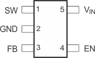
 Figure 5-1 DDC Package, DBV PackageSOT 5
PinsTop View
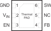
 Figure 5-2 DRV PackageWSON 6 PinsTransparent Top View
Table 5-1 Pin Functions
| PIN | I/O | DESCRIPTION | ||
|---|---|---|---|---|
| NAME | DDC, DBV NO. |
DRV NO. | ||
| EN | 4 | 3 | I | This is the enable pin of the device. Pulling this pin to ground forces the device into shutdown mode reducing the supply current to less than 1 μA. This pin should not be left floating and needs to be terminated. |
| FB | 3 | 4 | I | This is the feedback pin of the device. Connect this pin to the external voltage divider to program the desired output voltage. |
| GND | 2 | 1 | – | Ground |
| NC | – | 5 | – | No connection |
| SW | 1 | 6 | I | Connect the inductor and the Schottky diode to this pin. This is the switch pin and is connected to the drain of the internal power MOSFET. |
| VIN | 5 | 2 | I | Supply voltage pin |
| - | ThermalPAD | - | Solder to ground plane for heat sink | |