SLVS441D December 2002 – December 2014 TPS61042
PRODUCTION DATA.
- 1 Features
- 2 Applications
- 3 Description
- 4 Typical Application
- 5 Revision History
- 6 Pin Configuration and Functions
- 7 Specifications
- 8 Detailed Description
- 9 Application and Implementation
- 10Power Supply Recommendations
- 11Layout
- 12Device and Documentation Support
- 13Mechanical, Packaging, and Orderable Information
Package Options
Refer to the PDF data sheet for device specific package drawings
Mechanical Data (Package|Pins)
- DRB|8
Thermal pad, mechanical data (Package|Pins)
- DRB|8
Orderable Information
6 Pin Configuration and Functions
SON (DRB) Package
8 Pins
TOP VIEW
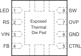
The exposed thermal die pad is connected to GND.
Pin Functions
| PIN | I/O | DESCRIPTION | |
|---|---|---|---|
| NAME | NO. | ||
| CTRL | 5 | I | Combined enable and PWM control pin. If CTRL is constantly pulled high, the device is enabled and the internal LED switch (Q2) is constantly turned on. When CTRL is pulled to GND, the device is disabled. Apply a PWM signal (100 Hz to 50 kHz) to this pin to control the brightness of the LEDs |
| FB | 4 | I | Feedback. FB regulates the LED current through the sense resistor by regulating the voltage across RS to 252 mV. |
| GND | 6 | GND | |
| LED | 1 | I | Input of the LED switch (Q2). Connect the LEDs to this pin. |
| OVP | 7 | I | Overvoltage protection. OVP is connected to the output capacitor of the converter. |
| RS | 2 | O | Output of the internal LED switch. The sense resistor that programs the LED current is connected to RS. |
| SW | 8 | I | Drain of the integrated switch (Q1) |
| VIN | 3 | I | Input supply pin. |