SLUS525A March 2007 – September 2015 TPS61050 , TPS61052
PRODUCTION DATA.
- 1 Features
- 2 Applications
- 3 Description
- 4 Revision History
- 5 Pin Configuration and Functions
- 6 Specifications
- 7 Detailed Description
-
8 Application and Implementation
- 8.1 Application Information
- 8.2
Typical Applications
- 8.2.1 Typical Application Schematic
- 8.2.2 High-Power White LED Solution Featuring Privacy Indicator
- 8.2.3 High-Power White LED Solution Featuring No-Latency Turn-Down Through PA TX Signal
- 8.2.4 High-Power White LED Flash Driver And AF/Zoom Motor Drive Supply
- 8.2.5 White LED Flash Driver and Audio Amplifier Power Supply Exclusive Operation
- 8.2.6 White LED Flash Driver and Audio Amplifier Power Supply Operating Simultaneously
- 8.2.7 White LED Flash Driver and Auxiliary Lighting Zone Power Supply
- 8.2.8 2 × 300 mA Dual LED Camera Flash
- 9 Power Supply Recommendations
- 10Layout
- 11Device and Documentation Support
- 12Mechanical, Packaging, and Orderable Information
Package Options
Mechanical Data (Package|Pins)
Thermal pad, mechanical data (Package|Pins)
- DRC|10
Orderable Information
6 Specifications
6.1 Absolute Maximum Ratings
over operating free-air temperature range (unless otherwise noted)(1)| MIN | MAX | UNIT | ||
|---|---|---|---|---|
| Voltage on AVIN, VOUT, SW, LED (2) | –0.3 | 7 | V | |
| Voltage on SCL, SDA, FLASH_SYNC, GPIO, ENVM (2) | –0.3 | 7 | V | |
| Input current on GPIO | 25 | mA | ||
| TA | Operating ambient temperature (3) | –40 | 85 | °C |
| TJ (MAX) | Maximum operating junction temperature | 150 | °C | |
| Tstg | Storage temperature | –65 | 150 | °C |
(1) Stresses beyond those listed under Absolute Maximum Ratings may cause permanent damage to the device. These are stress ratings only, which do not imply functional operation of the device at these or any other conditions beyond those indicated under Recommended Operating Conditions. Exposure to absolute-maximum-rated conditions for extended periods may affect device reliability.
(2) All voltage values are with respect to network ground terminal.
(3) In applications where high power dissipation and/or poor package thermal resistance is present, the maximum ambient temperature may have to be derated. Maximum ambient temperature (TA(max)) is dependent on the maximum operating junction temperature (TJ(max)), the maximum power dissipation of the device in the application (PD(max)), and the junction-to-ambient thermal resistance of the part/package in the application (θJA), as given by the following equation: TA(max)= TJ(max)–(θJA × PD(max)).
6.2 ESD Ratings
| VALUE | UNIT | |||
|---|---|---|---|---|
| V(ESD) | Electrostatic discharge | Human body model (HBM), per ANSI/ESDA/JEDEC JS-001(1) | ±2000 | V |
| Charged-device model (CDM), per JEDEC specification JESD22-C101(2) | ±1000 | |||
| Machine model (MM) | ±200 | |||
(1) JEDEC document JEP155 states that 500-V HBM allows safe manufacturing with a standard ESD control process.
(2) JEDEC document JEP157 states that 250-V CDM allows safe manufacturing with a standard ESD control process.
6.3 Recommended Operating Conditions
over operating free-air temperature range (unless otherwise noted)| MIN | NOM | MAX | UNIT | ||
|---|---|---|---|---|---|
| VIN | Input voltage range | 2.5 | 3.6 | 6 | V |
| VOUT | Output voltage range in Current regulator mode | VIN | 5.5 | V | |
| Output voltage range in Voltage regulator mode | 4.5 | 5.25 | |||
| L | Inductance effective value range | 1.3 | 2.2 | 2.9 | V |
| CIN | Input capacitance range | 10 | µH | ||
| COUT | Output capacitance effective value range | 3 | 10 | 50 | µF |
| TJ | Operating junction temperature | –40 | 125 | ||
6.4 Thermal Information
| THERMAL METRIC(1) | TPS6105x | UNIT | ||
|---|---|---|---|---|
| DRC (VSON) | YZG (DSBGA) | |||
| 10 PINS | 12 PINS | |||
| RθJA | Junction-to-ambient thermal resistance | 48.5 | 82 | °C/W |
| RθJC(top) | Junction-to-case (top) thermal resistance | 67.4 | 0.6 | °C/W |
| RθJB | Junction-to-board thermal resistance | 23 | 35 | °C/W |
| ψJT | Junction-to-top characterization parameter | 1.8 | 2.6 | °C/W |
| ψJB | Junction-to-board characterization parameter | 23.1 | 19.1 | °C/W |
| RθJC(bot) | Junction-to-case (bottom) thermal resistance | 5.3 | N/A | °C/W |
(1) For more information about traditional and new thermal metrics, see the Semiconductor and IC Package Thermal Metrics application report, SPRA953.
6.5 Electrical Characteristics
Unless otherwise noted the specification applies for VIN = 3.6 V over an operating junction temp. of –40°C ≤ TJ ≤ 125°C. Typical values are for TA = 25°C.| PARAMETER | TEST CONDITIONS | MIN | TYP | MAX | UNIT | |
|---|---|---|---|---|---|---|
| SUPPLY CURRENT | ||||||
| VIN | Input voltage | 2.5 | 6 | V | ||
| Minimum input voltage for start-up | MODE_CTRL[1:0] = 11, OV[1:0] = 01, RL = 10 Ω | 2.5 | V | |||
| IQ | Operating quiescent current into AVIN | MODE_CTRL[1:0] = 01, ILED = 0 mA | 8.5 | mA | ||
| ISD | Shutdown current into AVIN | MODE_CTRL[1:0] = 00, OV[1:0] ≠ 11 –40°C ≤ TJ ≤ 85°C |
0.3 | 3 | μA | |
| MODE_CTRL[1:0] = 00, OV[1:0] = 11 –40°C ≤ TJ ≤ 85°C |
140 | μA | ||||
| VUVLO | Undervoltage lockout threshold | VIN falling | 2.3 | 2.4 | V | |
| OUTPUT | ||||||
| VOUT | Output voltage | Current regulator mode | VIN | 5.5 | V | |
| Voltage regulator mode | 4.5 | 5.25 | ||||
| OVP | OVP Output overvoltage protection | VOUT rising | 5.7 | 6 | 6.25 | V |
| Output overvoltage protection hysterisis | 0.15 | V | ||||
| D | Minimum duty cycle | 7.5% | ||||
| LED current accuracy(1) | 0.25 V ≤ VLED ≤ 2 V, 50 mA ≤ ILED ≤ 250 mA, TJ = 50°C |
–15% | 15% | |||
| 0.25 V ≤ VLED ≤ 2 V, 200 mA ≤ ILED ≤ 1200 mA, TJ = 50°C |
–12% | 12% | ||||
| LED current temperature coefficient | 0.08 | %/°C | ||||
| DC output voltage accuracy | 2.5 V ≤ VIN ≤ 0.9 VOUT, PWM operation | –3% | 3% | |||
| VLED | LED sense voltage | ILED = 1200 mA | 250 | mV | ||
| LED input leakage current | VLED = VOUT = 5 V, –40°C ≤ TJ ≤ 85°C | 0.1 | 1 | μA | ||
| POWER SWITCH | ||||||
| rDS(on) | Switch MOSFET on-resistance | VOUT = VGS = 3.6 V | 80 | mΩ | ||
| Rectifier MOSFET on-resistance | 80 | |||||
| Ilkg(SW) | Switch MOSFET leakage | VDS = 6 V, –40°C ≤ TJ ≤ 85°C | 0.1 | 1 | μA | |
| Rectifier MOSFET leakage | 0.1 | 1 | ||||
| Ilim | Switch current limit | 2.5 V ≤ VIN ≤ 6 V, ILIM bits = 00 | 850 | 1000 | 1150 | mA |
| 2.5 V ≤ VIN ≤ 6 V, ILIM bits = 01, 10 (1) | 1275 | 1500 | 1725 | |||
| 2.5 V ≤ VIN ≤ 6 V, ILIM bits = 11 (1) | 1700 | 2000 | 2300 | |||
| Thermal shutdown(1) | 140 | 160 | °C | |||
| Thermal shutdown hysteresis(1) | 20 | °C | ||||
| OSCILLATOR | ||||||
| fSW | Oscillator frequency | 1.8 | 2 | 2.2 | MHz | |
| ADC | ||||||
| Resolution | 3 | Bits | ||||
| Total error(1) | VLED = 0.25 V, assured monotonic by design | ±0.25 | ±1 | LSB | ||
| SDA, SCL, GPIO, ENVM, FLASH_SYNC | ||||||
| V(IH) | High-level input voltage | 1.2 | V | |||
| V(IL) | Low-level input voltage | 0.4 | V | |||
| V(OL) | Low-level output voltage (SDA) | IOL = 8 mA | 0.3 | V | ||
| Low-level output voltage (GPIO) | DIR = 1, IOL = 8 mA | 0.3 | ||||
| I(LKG) | Logic input leakage current | Input connected to VIN or GND, –40°C ≤ TJ ≤ 85°C | 0.01 | 0.1 | μA | |
| GPIO pulldown resistance | DIR = 0, GPIO ≤ 0.4 V (TPS61050) | 400 | kΩ | |||
| ENVM pulldown resitance | ENVM ≤ 0.4 V (TPS61052) | 400 | kΩ | |||
| FLASH_SYNC pulldown resistance | FLASH_SYNC ≤ 0.4 V | 400 | kΩ | |||
| TIMING | ||||||
| Start-up time | From shutdown into torch mode ILED = 75 mA | 1.2 | ms | |||
| From shutdown into voltage mode through ENVM IOUT = 0 mA |
650 | μs | ||||
| LED current settling time(2) triggered by rising edge on FLASH_SYNC |
MODE_CTRL[1:0] = 10, ILED = from 0 mA to 900 mA |
400 | μs | |||
| LED current settling time(2) triggered by TX mask |
MODE_CTRL[1:0] = 10, ILED = 900 mA to 150 mA |
20 | μs | |||
(1) Assured by design. Not tested in production.
(2) Settling time to ±15% of the target value
6.6 I2C Interface Timing Characteristics(1)
| MIN | TYP | MAX | UNIT | |||
|---|---|---|---|---|---|---|
| fSCL | SCL clock frequency | Standard mode | 100 | kHz | ||
| Fast mode | 400 | |||||
| tBUF | Bus free time between a STOP and START condition | Standard mode | 4.7 | μs | ||
| Fast mode | 1.3 | |||||
| tHD; tSTA | Hold time (repeated) START condition | Standard mode | 4 | μs | ||
| Fast mode | 600 | ns | ||||
| tLOW | LOW period of the SCL clock | Standard mode | 4.7 | μs | ||
| Fast mode | 1.3 | |||||
| tHIGH | HIGH period of the SCL clock | Standard mode | 4 | μs | ||
| Fast mode | 600 | ns | ||||
| tSU; tSTA | Setup time for a repeated START condition | Standard mode | 4.7 | μs | ||
| Fast mode | 600 | ns | ||||
| tSU; tDAT | Data setup time | Standard mode | 250 | ns | ||
| Fast mode | 100 | |||||
| tHD; tDAT | Data hold time | Standard mode | 0 | 3.45 | μs | |
| Fast mode | 0 | 0.9 | ||||
| tRCL | Rise time of SCL signal | Standard mode | 20 + 0.1CB | 1000 | ns | |
| Fast mode | 20 + 0.1CB | 300 | ||||
| tRCL1 | Rise time of SCL signal after a repeated START condition and after an acknowledge bit | Standard mode | 20 + 0.1CB | 1000 | ns | |
| Fast mode | 20 + 0.1CB | 1000 | ||||
| tFCL | Fall time of SCL signal | Standard mode | 20 + 0.1CB | 300 | ns | |
| Fast mode | 20 + 0.1CB | 300 | ||||
| tRDA | Rise time of SDA signal | Standard mode | 20 + 0.1CB | 1000 | ns | |
| Fast mode | 20 + 0.1CB | 300 | ||||
| tFDA | Fall time of SDA signal | Standard mode | 20 + 0.1CB | 300 | ns | |
| Fast mode | 20 + 0.1CB | 300 | ||||
| tSU; tSTO | Setup time for STOP condition | Standard mode | 4 | μs | ||
| Fast mode | 600 | ns | ||||
| CB | Capacitive load for SDA and SCL | 400 | pF | |||
(1) Assured by design. Not tested in production.
 Figure 1. Serial Interface Timing For F/S-Mode
6.7 Typical Characteristics
Table 1. Table of Graphs
| GRAPH TITLE | FIGURE | |
|---|---|---|
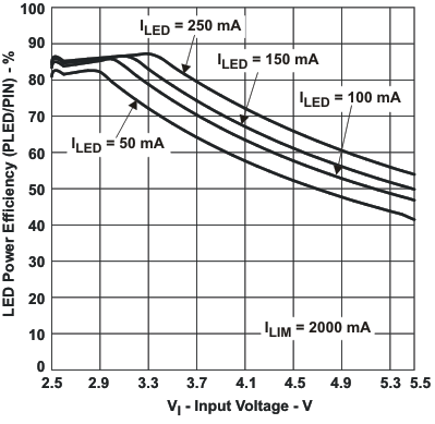
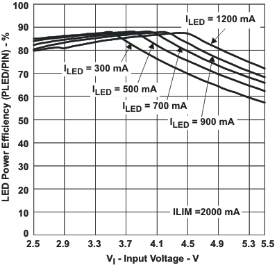
| LED Power Efficiency | vs Input Voltage | Figure 2, Figure 3 |
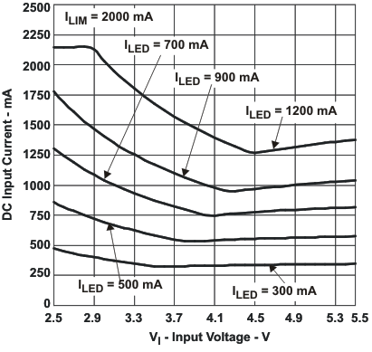
| DC Input Current | vs Input Voltage | Figure 4 |
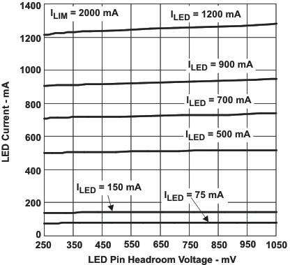
| LED Current | vs LED Pin Headroom Voltage | Figure 5 |
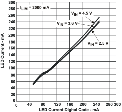
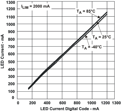
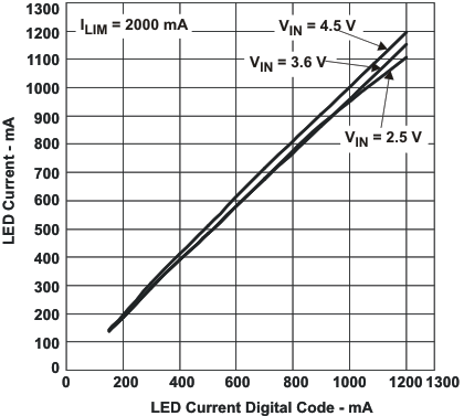
| LED Current | vs LED Current Digital Code | Figure 6, Figure 7, Figure 8 |
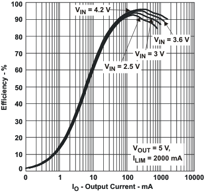
| Voltage Mode Efficiency | vs Output Current | Figure 9 |
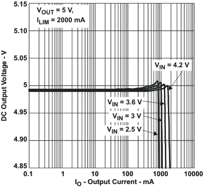
| DC Output Voltage | vs Load Current | Figure 10 |
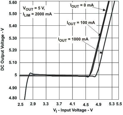
| DC Output Voltage | vs Input Voltage | Figure 11 |
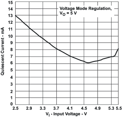
| Quiescent Current | vs Input Voltage | Figure 12 |
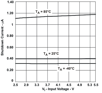
| Shutdown Current | vs Input Voltage | Figure 13 |
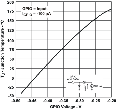
| Junction Temperature | vs GPIO Voltage | Figure 14 |
