SLVSCM8D May 2015 – August 2021 TPS61088
PRODUCTION DATA
- 1 Features
- 2 Applications
- 3 Description
- 4 Revision History
- 5 Pin Configuration and Functions
- 6 Specifications
- 7 Detailed Description
- 8 Application and Implementation
- 9 Power Supply Recommendations
- 10Layout
- 11Device and Documentation Support
- 12Mechanical, Packaging, and Orderable Information
Package Options
Mechanical Data (Package|Pins)
- RHL|20
Thermal pad, mechanical data (Package|Pins)
- RHL|20
Orderable Information
3 Description
The TPS61088 is a high-power density, fully-integrated synchronous boost converter with a 11-mΩ power switch and a 13-mΩ rectifier switch to provide a high efficiency and small size solution in portable systems. The TPS61088 has a wide input voltage range from 2.7 V to 12 V to support applications with single-cell or two-cell Lithium batteries. The device has 10-A switch current capability and is capable of providing an output voltage up to 12.6 V.
The TPS61088 uses adaptive constant off-time peak current control topology to regulate the output voltage. In moderate to heavy load condition, the TPS61088 works in pulse width modulation (PWM) mode. In light load condition, the device has two operation modes selected by the MODE pin. One is the pulse frequency modulation (PFM) mode to improve the efficiency and another one is forced PWM mode to avoid application problems caused by low switching frequency. The switching frequency in PWM mode is adjustable, ranging from 200 kHz to 2.2 MHz by an external resistor. The TPS61088 also implements a programmable soft-start function and an adjustable switching peak current limit function. In addition, the device provides 13.2-V output overvoltage protection, cycle-by-cycle overcurrent protection, and thermal shutdown protection.
The TPS61088 is available in a 4.50-mm × 3.50-mm 20-pin VQFN package.
| PART NUMBER | PACKAGE | BODY SIZE (NOM) |
|---|---|---|
| TPS61088 | VQFN (20) | 4.50 mm × 3.50 mm |
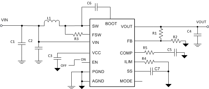
 Typical Application
Circuit