SNVSA40A October 2014 – March 2016 TPS61169
PRODUCTION DATA.
- 1 Features
- 2 Applications
- 3 Description
- 4 Simplified Schematic
- 5 Revision History
- 6 Pin Configuration and Functions
- 7 Specifications
- 8 Detailed Description
- 9 Application and Implementation
- 10Power Supply Recommendations
- 11Layout
- 12Device and Documentation Support
- 13Mechanical, Packaging, and Orderable Information
Package Options
Mechanical Data (Package|Pins)
- DCK|5
Thermal pad, mechanical data (Package|Pins)
Orderable Information
8 Detailed Description
8.1 Overview
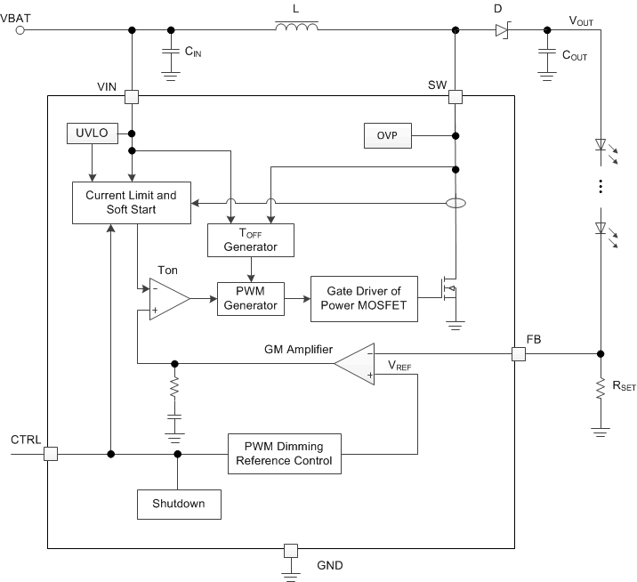
The TPS61169 is a high-efficiency, high-output voltage boost converter in small package size. The device integrates 40-V/1.8-A switch FET and is designed for output voltage up to 39 V with a switch peak current limit of 1.2 A minimum. Its large driving capability can drive single or parallel LED strings for small to large size panel backlighting.
The TPS61169 operates in a current mode scheme with quasi-constant frequency. It is internally compensated for maximum flexibility and stability. The switching frequency is 1.2 MHz, and the minimum input voltage is 2.7 V. During the on-time, the current rises into the inductor. When the current reaches a threshold value set by the internal GM amplifier, the power switch MOSFET is turned off. The polarity of the inductor changes and forward biases the schottky diode which lets the current flow towards the output of the boost converter. The off-time is fixed for a certain VIN and VOUT, and therefore maintains the same frequency when varying these parameters.
However, for different output loads, the frequency slightly changes due to the voltage drop across the RDS(ON) of the power switch MOSFET, this has an effect on the voltage across the inductor and thus on tON (tOFF remains fixed). The fixed off-time maintains a quasi-fixed frequency that provides better stability for the system over a wider range of input and output voltages than conventional boost converters. The TPS61169 topology has also the benefits of providing very good load and line regulations, and excellent line and load transient responses.
The feedback loop regulates the FB pin to a low reference voltage (204 mV typical), reducing the power dissipation in the current sense resistor.
8.2 Functional Block Diagram

8.3 Feature Description
8.3.1 Soft Start-Up
Soft-start circuitry is integrated into the IC to avoid high inrush current spike during start-up. After the device is enabled, the GM amplifier output voltage ramps up very slowly, which ensures that the output voltage rises slowly to reduce the input current. During this period, the switch current limit is set to 0.72 A. After around 6.5 ms, the switch current limit changes back to ILIM, and the FB pin voltage ramps up to the reference voltage slowly. These features ensure the smooth start-up and minimize the inrush current. See Figure 12 for a typical example.
8.3.2 Open LED Protection
Open LED protection circuitry prevents IC damage as the result of white LED disconnection. The TPS61169 monitors the voltage at the SW pin and FB pin during each switching cycle. The circuitry turns off the switch FET and shuts down the IC when both of the following conditions persist for 3 switching cycles: (1) the SW voltage exceeds the VOVP threshold, and (2) the FB voltage is less than 30 mV. As the result, the output voltage falls to the level of the input supply. The device remains in shutdown mode until it is enabled by toggling the CTRL pin.
8.3.3 Shutdown
The TPS61169 enters shutdown mode when the CTRL voltage is logic low for more than 2.5 ms. During shutdown, the input supply current for the device is less than 2 μA (max). Although the internal switch FET does not switch in shutdown, there is still a DC current path between the input and the LEDs through the inductor and Schottky diode. The minimum forward voltage of the LED array must exceed the maximum input voltage to ensure that the LEDs remain off in shutdown.
8.3.4 Current Program
The FB voltage is regulated by a low 204-mV reference voltage. The LED current is programmed externally using a current-sense resistor in series with the LED string(s). The value of the RSET is calculated using:

where
- ILED = total output current of LED string(s)
- VFB = regulated voltage of FB pin
- RSET = current sense resistor
The output current tolerance depends on the FB accuracy and the current sensor resistor accuracy.
8.3.5 LED Brightness Dimming
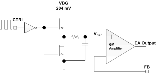
The TPS61169 receives PWM dimming signal at CTRL pin to control the total output current. When the CTRL pin is constantly high, the FB voltage is regulated to 204 mV typically. When the duty cycle of the input PWM signal is low, the regulation voltage at FB pin is reduced, and the total output current is reduced; therefore, it achieves LED brightness dimming. The relationship between the duty cycle and FB regulation voltage is given by:

where
- Duty = Duty cycle of the PWM signal
- 204 mV = internal reference voltage
Thus, the user can easily control the WLED brightness by controlling the duty cycle of the PWM signal.
As shown in Figure 3, the IC chops up the internal 204-mV reference voltage at the duty cycle of the PWM signal. The pulse signal is then filtered by an internal low-pass filter. The output of the filter is connected to the GM amplifier as the reference voltage for the FB pin regulation. Therefore, although a PWM signal is used for brightness dimming, only the WLED DC current is modulated, which is often referred as analog dimming. This eliminates the audible noise which often occurs when the LED current is pulsed in replica of the frequency and duty cycle of PWM control. Unlike other methods which filter the PWM signal for analog dimming, TPS61169 regulation voltage is independent of the PWM logic voltage level which often has large variations.
For optimum performance, use the PWM dimming frequency in the range of 5 kHz to 100 kHz. If the PWM frequency is lower than 5 kHz, it is out of the low pass filter's filter range, the FB regulation voltage ripple becomes large, causing large output ripple and may generate audible noise.
 Figure 3. Programmable FB Voltage Using PWM Signal
8.3.6 Undervoltage Lockout
An undervoltage lockout prevents operation of the device at input voltages below typical 2 V. When the input voltage is below the undervoltage threshold, the device is shut down, and the internal switch FET is turned off. If the input voltage rises by undervoltage lockout hysteresis, the IC restarts.
8.3.7 Thermal Foldback and Thermal Shutdown
When TPS61169 drives heavy load for large size panel applications, the power dissipation increases a lot and the device junction temperature may reach a very high value, affecting the device function and reliability. In order to lower the thermal stress, the TPS61169 features a thermal foldback function. When the junction temperature is higher than 100°C, the switch current limit ILIM is reduced automatically as Figure 2 shows. This thermal foldback mechanism controls the power dissipation and keeps the junction temperature from rising to a very high value. If the typical junction temperature of 160°C is exceeded, an internal thermal shutdown turns off the device. The device is released from shutdown automatically when the junction temperature decreases by 15°C.
8.4 Device Functional Modes
8.4.1 Operation With CTRL
The enable rising edge threshold voltage is 1.2 V. When the CTRL pin is held below that voltage the device is disabled and switching is inhibited. The IC quiescent current is reduced in this state. When input voltage is above the UVLO threshold, and the CTRL pin voltage is increased above the rising edge threshold, the device becomes active. Switching enables, and the soft-start sequence initiates.