SNVSAF5D January 2016 – May 2021 TPS61194
PRODUCTION DATA
- 1 Features
- 2 Applications
- 3 Description
- 4 Revision History
- 5 Pin Configuration and Functions
-
6 Specifications
- 6.1 Absolute Maximum Ratings
- 6.2 ESD Ratings
- 6.3 Recommended Operating Conditions
- 6.4 Thermal Information
- 6.5 Electrical Characteristics (1) (1)
- 6.6 Internal LDO Electrical Characteristics
- 6.7 Protection Electrical Characteristics
- 6.8 Current Sinks Electrical Characteristics
- 6.9 PWM Brightness Control Electrical Characteristics
- 6.10 Boost and SEPIC Converter Characteristics
- 6.11 Logic Interface Characteristics
- 6.12 Typical Characteristics
- 7 Detailed Description
- 8 Application and Implementation
- 9 Power Supply Recommendations
- 10Layout
- 11Device and Documentation Support
- 12Mechanical, Packaging, and Orderable Information
Package Options
Mechanical Data (Package|Pins)
- PWP|20
Thermal pad, mechanical data (Package|Pins)
- PWP|20
Orderable Information
8.2.1.2.1 Inductor Selection
There are two main considerations when choosing an inductor; the inductor must not saturate, and the inductor current ripple must be small enough to achieve the desired output voltage ripple. Different saturation current rating specifications are followed by different manufacturers so attention must be given to details. Saturation current ratings are typically specified at 25°C. However, ratings at the maximum ambient temperature of application should be requested from the manufacturer. Shielded inductors radiate less noise and are preferred. The saturation current must be greater than the sum of the maximum load current, and the worst case average-to-peak inductor current. Equation 4 shows the worst case conditions
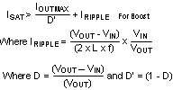
- IRIPPLE - peak inductor current
- IOUTMAX - maximum load current
- VIN - minimum input voltage in application
- L - min inductor value including worst case tolerances
- f - minimum switching frequency
- VOUT - output voltage
- D - Duty Cycle for CCM Operation
As a result, the inductor should be selected according to the ISAT. A more conservative and recommended approach is to choose an inductor that has a saturation current rating greater than the maximum current limit. A saturation current rating of at least 2.5 A is recommended for most applications. See Table 7-2 for recommended inductance value for the different switching frequency ranges. The inductor’s resistance should be less than
300 mΩ for good efficiency.
See detailed information in Understanding Boost Power Stages in Switch Mode Power Supplies. Power Stage Designer™ Tool can be used for the boost calculation: http://www.ti.com/tool/powerstage-designer.