SLVSAN3B December 2010 – November 2016 TPS61199
PRODUCTION DATA.
- 1 Features
- 2 Applications
- 3 Description
- 4 Revision History
- 5 Pin Configuration and Functions
- 6 Specifications
- 7 Detailed Description
- 8 Application and Implementation
- 9 Power Supply Recommendations
- 10Layout
- 11Device and Documentation Support
- 12Mechanical, Packaging, and Orderable Information
Package Options
Mechanical Data (Package|Pins)
Thermal pad, mechanical data (Package|Pins)
- PWP|20
Orderable Information
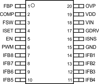
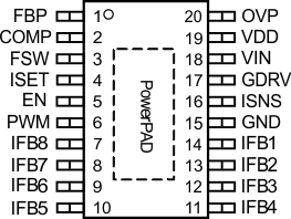
5 Pin Configuration and Functions
NS Package
20-Pin SO
Top View

PWP Package
20-Pin HTSSOP
Top View

Pin Functions
| PIN | TYPE | DESCRIPTION | |
|---|---|---|---|
| NAME | NO. | ||
| COMP | 2 | Output | Loop compensation pin. Connect an RC network to make loop stable (see Loop Consideration ). |
| EN | 5 | Input | Enable/disable pin — high = device is enabled; low = device is disabled. |
| FBP | 1 | Output | LED short-across protection threshold program pin (see Protection) |
| FSW | 3 | Output | Boost switching frequency selection pin. Connect a resistor to set the frequency between 300 kHz to 800 kHz. |
| GDRV | 17 | Output | External Switch MOSFET gate driver output pin |
| GND | 15 | Ground | Ground pin |
| IFB1 to IFB8 | 7, 8, 9, 10, 11 12, 13, 14 |
Input | Regulated current sink input pins. |
| ISET | 4 | Output | Full-scale LED current selection pin; connect a resistor to program LED current for each string |
| ISNS | 16 | Input | External MOSFET current sense positive input pin |
| OVP | 20 | Input | Overvoltage protection pin (see Protection) |
| PWM | 6 | Input | PWM dimming signal input pin. The frequency must be in the range of 100 Hz to 22 kHz. |
| VDD | 19 | Output | Internal regulator output pin. Connect a 2.2-μF capacitor between this pin to GND. |
| VIN | 18 | Input | Supply input pin. This pin can be tied to a voltage different from the power stage input. |
| PowerPAD – HTTSOP package | — | The PowerPAD pad must be soldered to the ground. If possible, use thermal vias to connect to top and internal ground plane layers for ideal power dissipation. | |