SLVSA99C May 2011 – April 2018 TPS61260 , TPS61261
PRODUCTION DATA.
- 1 Features
- 2 Applications
- 3 Description
- 4 Revision History
- 5 Pin Configuration and Functions
- 6 Specifications
- 7 Parameter Measurement Information
- 8 Detailed Description
- 9 Application and Implementation
- 10Power Supply Recommendations
- 11Layout
- 12Device and Documentation Support
- 13Mechanical, Packaging, and Orderable Information
Package Options
Mechanical Data (Package|Pins)
- DRV|6
Thermal pad, mechanical data (Package|Pins)
- DRV|6
Orderable Information
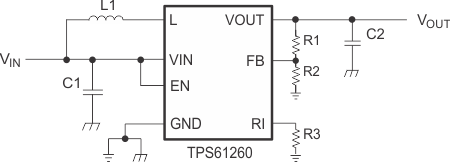
8.5.1 Programming the Output Voltage
Within the TPS6126x family, there are fixed and adjustable output voltage versions available. To properly configure the fixed output voltage devices, the FB pin is used to sense the output voltage. This means that it must be connected directly to VOUT. For the adjustable output voltage version, an external resistor divider is used to adjust the output voltage. The resistor divider must be connected between the VOUT, FB, and GND pins. When the output voltage is regulated properly, the typical value of the voltage at the FB pin is 500 mV. The maximum recommended value for the output voltage is 4.0 V. The current through the resistive divider should be about 100 times greater than the current into the FB pin. The typical current into the FB pin is 0.01 μA, and the voltage across the resistor between the FB and GND pins, R2, is typically 500 mV. Based on these two values, the recommended value for R2 should be lower than 500 kΩ, in order to set the divider current at 1 μA or higher. It is also recommended to keep the total value for the resistor divider, R1 + R2, in the range of 1 MΩ. From that, the value of the resistor connected between VOUT and FB, R1, depending on the needed output voltage (VOUT), can be calculated using Equation 1:

 Figure 17. Typical Application Circuit for Adjustable Output Voltage Option