SLVS978D March 2010 – September 2016 TPS61310 , TPS61311
PRODUCTION DATA.
- 1 Features
- 2 Applications
- 3 Description
- 4 Revision History
- 5 Device Comparison Table
- 6 Pin Configuration and Functions
- 7 Specifications
- 8 Parameter Measurement Information
-
9 Detailed Description
- 9.1 Overview
- 9.2 Functional Block Diagram
- 9.3
Feature Description
- 9.3.1 Privacy Indicator
- 9.3.2
Safe Operation and Protection Features
- 9.3.2.1 LED Temperature Monitoring (Finger-Burn Protection)
- 9.3.2.2 LED Failure Modes (Open and Short Detection) and Overvoltage Protection
- 9.3.2.3 LED Current Ramp-Up and Ramp-Down
- 9.3.2.4 Battery Voltage Droop Monitoring and Protection
- 9.3.2.5 Undervoltage Lockout
- 9.3.2.6 Hot Die Detection and Thermal Shutdown
- 9.3.2.7 Current Limit
- 9.3.2.8 Flash Blanking (Tx-Mask) for Instantaneous Flash Current Reduction
- 9.3.3 Start-Up Sequence
- 9.3.4 NRESET Input: Hardware Enable or Disable
- 9.3.5 Serial Interface Description
- 9.3.6 LED Forward Voltage Calibration
- 9.4 Device Functional Modes
- 9.5 Register Maps
- 10Application and Implementation
- 11Power Supply Recommendations
- 12Layout
- 13Device and Documentation Support
- 14Mechanical, Packaging, and Orderable Information
Package Options
Mechanical Data (Package|Pins)
- YFF|20
Thermal pad, mechanical data (Package|Pins)
Orderable Information
1 Features
- Operational Modes:
- Video Light and Flash Strobe
- Voltage Regulated Converter: 3.8 V to 5.7 V With Down Mode
- Standby: 2 µA (Typical)
- LED VF Measurement
- Power-Save Mode for Improved Efficiency at Low Output Power, Up to 95% Efficiency
- I2C Compatible Interface up to 3.4 Mbps
- Dual Wire Camera Module Interface
- Zero Latency Tx-Masking Input
- Hardware Reset Input
- Privacy Indicator LED Output
- GPIO and Power Good Output
- Various Safe Operation and Robust Handling Features:
- LED Temperature Monitoring
- Open and Shorted LED Detection and Protection
- Integrated LED Safety Timer
- Automatic Battery Voltage Droop Monitoring and Protection
- Smooth LED Current Ramp-Up and Ramp-Down
- Undervoltage Lockout
- Total Solution Size of Less Than 25 mm2
- Available in a 20-Pin NanoFree™ DSBGA Package
2 Applications
- Single, Dual, or Triple White LED Flash Supply for Cell Phones and Smart-Phones
- Video Lighting for Digital Video Applications
- General Lighting Applications
- Audio Amplifier Power Supply
3 Description
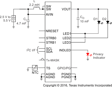
The TPS6131x family is an integrated solution with a wide feature set for driving up to three LEDs for still-camera flash strobe and video-camera lighting applications. It is based on a high efficiency synchronous boost topology with combinable current sinks to drive up to three white LEDs in parallel. The 2-MHz switching frequency allows the use of small and low-profile 2.2-µH inductors. To optimize overall efficiency, the device operates with a low LED-feedback voltage and regulated output-voltage adaptation.
The device integrates a control scheme that automatically optimizes the LED current flash budget as a function of the battery voltage condition.
The TPS6131x not only operates as a regulated current source, but also as a standard voltage boost regulator. The device enters power-save mode operation at light load currents to maintain high efficiency over the entire load current range. These operating modes can be useful to supply other high power devices in the system (for example, a hands-free audio PA).
To simplify video light and flash synchronization with the camera module, the device offers a dedicated control interface (STRB0, STRB1) for zero latency LED turnon time.
Device Information(1)
| PART NUMBER | PACKAGE | BODY SIZE (NOM) |
|---|---|---|
| TPS61310, TPS61311 | DSBGA (20) | 2.20 mm × 1.90 mm |
- For all available packages, see the orderable addendum at the end of the data sheet.
Typical Application

4 Revision History
Changes from C Revision (November 2012) to D Revision
- Added Device Information table,ESD Ratings table,Recommended Operating Conditions table,Thermal Information table,Device and Documentation Support section, and Mechanical, Packaging, and Orderable Information sectionGo
- Deleted Ordering Information table; see POA at the end of the data sheetGo
Changes from B Revision (September 2011) to C Revision
- Added revision letter C to literature numberGo
- Added TPS61311 to ordering tableGo
- Added Current Limit Setting for TPS61311Go
- Added current limit setting for TPS61311 in register mapGo
Changes from A Revision (October 2010) to B Revision