SLVSAJ0F November   2011  – October 2021 TPS62140 , TPS62140A , TPS62141 , TPS62142 , TPS62143

PRODUCTION DATA  

  1. Features
  2. Applications
  3. Description
  4. Revision History
  5. Device Comparison Table
  6. Pin Configuration and Functions
  7. Specifications
    1. 7.1 Absolute Maximum Ratings (1)
    2. 7.2 ESD Ratings
    3. 7.3 Recommended Operating Conditions
    4. 7.4 Thermal Information
    5. 7.5 Electrical Characteristics
    6. 7.6 Typical Characteristics
  8. Detailed Description
    1. 8.1 Overview
    2. 8.2 Functional Block Diagrams
    3. 8.3 Feature Description
      1. 8.3.1 Enable/Shutdown (EN)
      2. 8.3.2 Soft-Start/Tracking (SS/TR)
      3. 8.3.3 Power Good (PG)
      4. 8.3.4 Pin-Selectable Output Voltage (DEF)
      5. 8.3.5 Frequency Selection (FSW)
      6. 8.3.6 Undervoltage Lockout (UVLO)
      7. 8.3.7 Thermal Shutdown
    4. 8.4 Device Functional Modes
      1. 8.4.1 Pulse-Width Modulation (PWM) Operation
      2. 8.4.2 Power Save Mode Operation
      3. 8.4.3 100% Duty-Cycle Operation
      4. 8.4.4 Current Limit and Short Circuit Protection
  9. Application and Implementation
    1. 9.1 Application Information
    2. 9.2 Typical Application
      1. 9.2.1 Design Requirements
      2. 9.2.2 Detailed Design Procedure
        1. 9.2.2.1 Programming the Output Voltage
        2. 9.2.2.2 External Component Selection
          1. 9.2.2.2.1 Inductor Selection
          2. 9.2.2.2.2 Capacitor Selection
            1. 9.2.2.2.2.1 Output Capacitor
            2. 9.2.2.2.2.2 Input Capacitor
            3. 9.2.2.2.2.3 Soft-Start Capacitor
        3. 9.2.2.3 Tracking Function
        4. 9.2.2.4 Output Filter and Loop Stability
      3. 9.2.3 Application Curves
    3. 9.3 System Examples
      1. 9.3.1 LED Power Supply
      2. 9.3.2 Active Output Discharge
      3. 9.3.3 Inverting Power Supply
      4. 9.3.4 Various Output Voltages
  10. 10Power Supply Recommendations
  11. 11Layout
    1. 11.1 Layout Guidelines
    2. 11.2 Layout Example
    3. 11.3 Thermal Considerations
  12. 12Device and Documentation Support
    1. 12.1 Device Support
      1. 12.1.1 Third-Party Products Disclaimer
    2. 12.2 Documentation Support
      1. 12.2.1 Related Documentation
    3. 12.3 Receiving Notification of Documentation Updates
    4. 12.4 Support Resources
    5. 12.5 Trademarks
    6. 12.6 Electrostatic Discharge Caution
    7. 12.7 Glossary
  13. 13Mechanical, Packaging, and Orderable Information

Package Options

Mechanical Data (Package|Pins)
Thermal pad, mechanical data (Package|Pins)
Orderable Information

Power Save Mode Operation

The TPS6214x enters its built-in power-save mode seamlessly if the load current decreases. This secures a high efficiency in light-load operation. The device remains in power-save mode as long as the inductor current is discontinuous.

In power-save mode, the switching frequency decreases linearly with the load current, maintaining high efficiency. The transition into and out of power-save mode happens within the entire regulation scheme and is seamless in both directions.

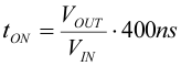
TPS6214x includes a fixed-on-time circuit. An estimate for this on-time, in steady-state operation with FSW = low, is:

Equation 1. GUID-569D7E9E-2F39-4910-9173-ADDC5D5AE16D-low.gif

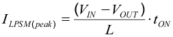
For very small output voltages, an absolute minimum on-time of about 80 ns is kept to limit switching losses. The operating frequency is thereby reduced from its nominal value, which keeps efficiency high. Also the off-time can reach its minimum value at high duty cycles. The output voltage remains regulated in such case. Using tON, the typical peak inductor current in Power Save Mode can be approximated by:

Equation 2. GUID-398EF72A-6D01-4A37-8193-29A48746131B-low.gif

When VIN decreases to typically 15% above VOUT, the TPS6214x does not enter power-save mode, regardless of the load current. The device maintains output regulation in PWM mode.