SLVSCH9E December   2014  – March 2022 TPS62406-Q1 , TPS62407-Q1 , TPS62422-Q1 , TPS62423-Q1 , TPS62424-Q1

PRODUCTION DATA  

  1. Features
  2. Applications
  3. Description
  4. Revision History
  5. Device Comparison Table
  6. Pin Configuration and Functions
  7. Specifications
    1. 7.1 Absolute Maximum Ratings
    2. 7.2 ESD Ratings
    3. 7.3 Recommended Operating Conditions
    4. 7.4 Thermal Information
    5. 7.5 Electrical Characteristics
    6. 7.6 Timing Requirements
    7. 7.7 Switching Characteristics
    8. 7.8 Typical Characteristics
  8. Detailed Description
    1. 8.1 Overview
      1. 8.1.1 Converter 1
      2. 8.1.2 Converter 2
    2. 8.2 Functional Block Diagram
    3. 8.3 Feature Description
      1. 8.3.1 Enable
      2. 8.3.2 DEF_1 Pin Function
      3. 8.3.3 180° Out-of-Phase Operation
      4. 8.3.4 Short-Circuit Protection
      5. 8.3.5 Thermal Shutdown
      6. 8.3.6 EasyScale Interface: One-Pin Serial Interface for Dynamic Output-Voltage Adjustment
        1. 8.3.6.1 General
        2. 8.3.6.2 Protocol
    4. 8.4 Device Functional Modes
      1. 8.4.1 Power-Save Mode
        1. 8.4.1.1 Dynamic Voltage Positioning
        2. 8.4.1.2 Soft Start
        3. 8.4.1.3 100% Duty-Cycle Low-Dropout Operation
        4. 8.4.1.4 Undervoltage Lockout
      2. 8.4.2 Mode Selection
    5. 8.5 Programming
      1. 8.5.1 Addressable Registers
        1. 8.5.1.1 Bit Decoding
        2. 8.5.1.2 Acknowledge
        3. 8.5.1.3 Mode Selection
  9. Application and Implementation
    1. 9.1 Application Information
      1. 9.1.1 Application Information
    2. 9.2 Typical Application
      1. 9.2.1 Design Requirements
      2. 9.2.2 Detailed Design Procedure
        1. 9.2.2.1 Output Voltage Setting
          1. 9.2.2.1.1 Converter 1 Fixed Default Output-Voltage Setting
          2. 9.2.2.1.2 Converter 2 Fixed Default Output-Voltage Setting
        2. 9.2.2.2 Output Filter Design (Inductor and Output Capacitor)
          1. 9.2.2.2.1 Inductor Selection
          2. 9.2.2.2.2 Output-Capacitor Selection
          3. 9.2.2.2.3 Input Capacitor Selection
      3. 9.2.3 Application Curves
    3. 9.3 System Examples
  10. 10Power Supply Recommendations
  11. 11Layout
    1. 11.1 Layout Guidelines
    2. 11.2 Layout Example
  12. 12Device and Documentation Support
    1. 12.1 Support Resources
    2. 12.2 Receiving Notification of Documentation Updates
    3. 12.3 Trademarks
    4. 12.4 Electrostatic Discharge Caution
    5. 12.5 Glossary
  13. 13Mechanical, Packaging, and Orderable Information

Package Options

Mechanical Data (Package|Pins)
Thermal pad, mechanical data (Package|Pins)
Orderable Information

Description

The TPS624xx-Q1 family of devices are synchronous dual step-down DC-DC converters for Automotive applications such as Advanced Driver Assistance Systems (ADAS). They provide two independent output voltage rails powered by a standard 3.3-V or 5-V voltage rail, with fixed output voltages optimized for powering the CMOS imager or serializer-deserializer in ADAS camera modules.

The EasyScale™ serial interface allows output-voltages modification during operation. The fixed-output-voltage versions TPS624xx-Q1 support one-pin-controlled simple dynamic voltage scaling for low-power processors.

The TPS624xx-Q1 family of devices operates at 2.25-MHz fixed switching frequency and enters the power-save mode operation at light load currents to maintain high efficiency over the entire load-current range. For low-noise applications, one can force the devices into fixed-frequency PWM mode by pulling the MODE/DATA pin high. The shutdown mode reduces the current consumption to 1.2-μA, typical. The devices allow the use of small inductors and capacitors to achieve a small solution size.

Device Information(1)
PART NUMBERPACKAGEBODY SIZE (NOM)
TPS62406-Q1VSON (10)3.00 mm × 3.00 mm
TPS62407-Q1
TPS62422-Q1
TPS62423-Q1
TPS62424-Q1
For all available packages, see the orderable addendum at the end of the datasheet.
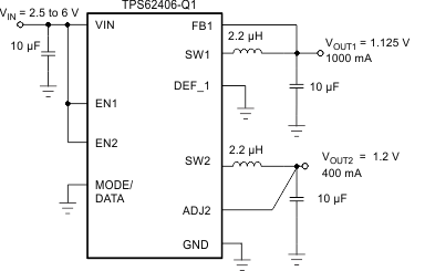
GUID-578B43C7-597E-4287-8358-021A5FE67C1F-low.gifSimplified Schematic
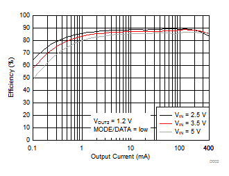
GUID-CA5194FC-135F-470A-AF05-9C6B823A9463-low.gifTPS62406-Q1 Efficiency vs Output Current, VOUT2