SLVSAO5B December 2010 – October 2015 TPS62590-Q1
PRODUCTION DATA.
- 1 Features
- 2 Applications
- 3 Description
- 4 Revision History
- 5 Pin Configuration and Functions
- 6 Specifications
- 7 Parameter Measurement Information
- 8 Detailed Description
- 9 Application and Implementation
- 10Power Supply Recommendations
- 11Layout
- 12Device and Documentation Support
- 13Mechanical, Packaging, and Orderable Information
Package Options
Mechanical Data (Package|Pins)
- DRV|6
Thermal pad, mechanical data (Package|Pins)
- DRV|6
Orderable Information
11 Layout
11.1 Layout Guidelines
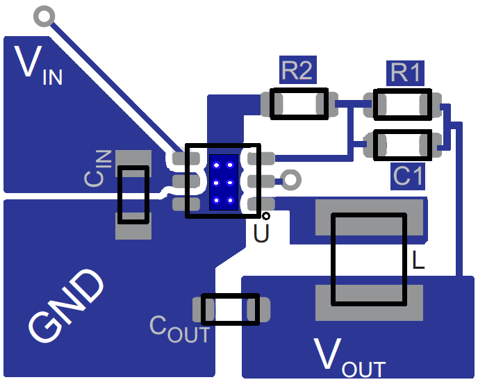
As for all switching power supplies, the layout is an important step in the design. Proper function of the device demands careful attention to PCB layout. Care must be taken in board layout to get the specified performance. If the layout is not carefully done, the regulator could show poor line and/or load regulation, stability issues, and EMI problems.
The following list details some generic layout guidelines for the TPS62590-Q1 device:
- It is critical to provide a low-inductance, low-impedance ground path and hence use wide and short traces for the main current paths.
- The input capacitor, output capacitor, and inductor should be placed as close as possible to the IC pins.
- Connect the GND pin of the device to the thermal pad of the PCB and use this pad as a star point.
- Use a common power GND node and a different node for the signal GND to minimize the effects of ground noise. Connect these ground nodes together at the thermal pad (star point) underneath the IC.
- Keep the traces to the GND pin, coming from small-signal components and the high current of the output capacitors, as short as possible to avoid ground noise.
- The output feedback line should be connected close to the output capacitor and routed away from noisy components and traces (for example, the SW line).
- Trace to the FB pin from voltage divider resistors center point should be as short as possible and should be away from noise sources, such as the inductor or the SW line.
- Add multiple thermal via's on the device thermal pad for better thermal performance.
11.2 Layout Example
 Figure 29. Layout