SLVSC68A June   2015  – June 2015 TPS62745 , TPS627451

PRODUCTION DATA.  

  1. Features
  2. Applications
  3. Description
  4. Typical Application Schematic
  5. Device Comparison Table
  6. Pin Configuration and Functions
  7. Specifications
    1. 7.1 Absolute Maximum Ratings
    2. 7.2 ESD Ratings
    3. 7.3 Recommended Operating Conditions
    4. 7.4 Thermal Information
    5. 7.5 Electrical Characteristics
    6. 7.6 Timing Characteristics
    7. 7.7 Typical Characteristics
  8. Detailed Description
    1. 8.1 Overview
    2. 8.2 Functional Block Diagram
    3. 8.3 Feature Description
      1. 8.3.1 DCS-Control™
      2. 8.3.2 Enable / Shutdown
      3. 8.3.3 Power Good Output (PG)
      4. 8.3.4 Output Voltage Selection (VSEL1 - 4)
      5. 8.3.5 Input Voltage Switch
    4. 8.4 Device Functional Modes
      1. 8.4.1 Soft Start
    5. 8.5 VOUT Discharge
    6. 8.6 Internal Current Limit
  9. Application and Implementation
    1. 9.1 Application Information
    2. 9.2 Typical Application
      1. 9.2.1 Design Requirements
      2. 9.2.2 Detailed Design Procedure
        1. 9.2.2.1 Output Voltage Selection (VSEL1 - 4)
        2. 9.2.2.2 Output Filter Design (Inductor and Output Capacitor)
        3. 9.2.2.3 Inductor Selection
        4. 9.2.2.4 DC/DC Output Capacitor Selection
        5. 9.2.2.5 Input Capacitor Selection
      3. 9.2.3 Application Curves
    3. 9.3 System Examples
      1. 9.3.1 TPS62745 Set to a Fixed Voltage of 3.3 V
        1. 9.3.1.1 Design Requirements
        2. 9.3.1.2 Detailed Design Procedure
        3. 9.3.1.3 Application Curves
      2. 9.3.2 Dynamic Voltage Change on TPS62745
        1. 9.3.2.1 Design Requirements
        2. 9.3.2.2 Detailed Design Procedure
        3. 9.3.2.3 Application Curves
  10. 10Power Supply Recommendations
  11. 11Layout
    1. 11.1 Layout Guidelines
    2. 11.2 Layout Example
  12. 12Device and Documentation Support
    1. 12.1 Device Support
      1. 12.1.1 Third-Party Products Disclaimer
    2. 12.2 Related Links
    3. 12.3 Community Resources
    4. 12.4 Trademarks
    5. 12.5 Electrostatic Discharge Caution
    6. 12.6 Glossary
  13. 13Mechanical, Packaging, and Orderable Information

Package Options

Mechanical Data (Package|Pins)
Thermal pad, mechanical data (Package|Pins)
Orderable Information

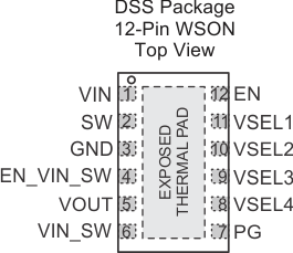
6 Pin Configuration and Functions

TPS62745 TPS627451 TPS62745_pinout_2x3_DSS_V12.gif

Pin Functions

PIN I/O DESCRIPTION
NAME NO.
VIN 1 PWR VIN power supply pin. Connect this pin close to the VIN terminal of the input capacitor. A ceramic capacitor of 4.7 µF from this pin to GND is required.
SW 2 OUT This is the switch pin which is connected to the internal MOSFET switches. Connect the inductor to this terminal.
GND 3 PWR GND supply pin. Connect this pin close to the GND terminal of the input and output capacitor.
EN_VIN_SW 4 IN This pin connects / disconnects the internal switch from VIN to pin VIN_SW. With EN_VIN_SW = Low, the switch is open. With EN_VIN_SW = High, the switch is closed connecting VIN with VIN_SW. If not used, the pin should be tied to GND.
VOUT 5 IN Feedback pin for the internal feedback divider network and regulation loop. Connect this pin directly to the output capacitor with a short trace.
VIN_SW 6 OUT This is the output of a switch connecting VIN with VIN_SW when EN_VIN_SW = High. If not used, leave this pin open.
PG 7 OUT This is an open drain power good output.
VSEL4 8 IN Output voltage selection pins. See Table 1 and Table 2 for VOUT selection. These pins must be terminated.
VSEL3 9 IN
VSEL2 10 IN
VSEL1 11 IN
EN 12 IN High level enables the devices, low level turns the device into shutdown mode. This pin must be terminated.
EXPOSED THERMAL PAD NC Not electrically connected to the IC. Connect this pad to GND and use it as a central GND plane.

Table 1. Output Voltage Setting for TPS62745

Device VOUT / V VSEL4 VSEL 3 VSEL 2 VSEL 1
TPS62745 1.8 0 0 0 0
1.9 0 0 0 1
2.0 0 0 1 0
2.1 0 0 1 1
2.2 0 1 0 0
2.3 0 1 0 1
2.4 0 1 1 0
2.5 0 1 1 1
2.6 1 0 0 0
2.7 1 0 0 1
2.8 1 0 1 0
2.9 1 0 1 1
3.0 1 1 0 0
3.1 1 1 0 1
3.2 1 1 1 0
3.3 1 1 1 1

Table 2. Output Voltage Setting for TPS627451

Device VOUT / V VSEL4 VSEL 3 VSEL 2 VSEL 1
TPS627451 1.3 0 0 0 0
1.4 0 0 0 1
1.5 0 0 1 0
1.6 0 0 1 1
1.7 0 1 0 0
1.8 0 1 0 1
1.9 0 1 1 0
2.0 0 1 1 1
2.1 1 0 0 0
2.2 1 0 0 1
2.3 1 0 1 0
2.4 1 0 1 1
2.5 1 1 0 0
2.6 1 1 0 1
2.7 1 1 1 0
2.8 1 1 1 1