SLVSD27B June 2015 – March 2021 TPS62746
PRODUCTION DATA
- 1 Features
- 2 Applications
- 3 Description
- 4 Revision History
- 5 Device Comparison Table
- 6 Pin Configuration and Functions
- 7 Specifications
- 8 Detailed Description
- 9 Application and Implementation
- 10Power Supply Recommendations
- 11Layout
- 12Device and Documentation Support
- 13Mechanical, Packaging, and Orderable Information
Package Options
Refer to the PDF data sheet for device specific package drawings
Mechanical Data (Package|Pins)
- YFP|8
Thermal pad, mechanical data (Package|Pins)
Orderable Information
3 Description
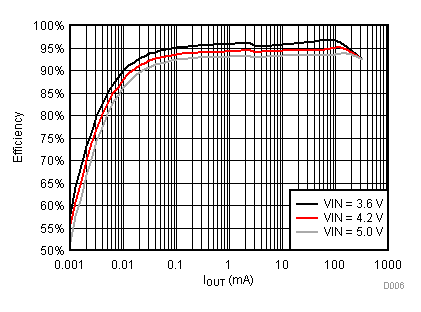
The TPS62746 is a high efficiency step down converter with ultra low quiescent current of typical 360 nA. The device is optimized to operate with a 2.2-µH inductor and 10µF output capacitor. The device uses DCS-Control™ and operates with a typical switching frequency of 1.2 MHz. In Power Save Mode the device extends the light load efficiency down to a load current range of 10-µA and below. TPS62746 provides an output current of 300 mA. Once started the device operates down to an input voltage range of 2.0 V. This allows to operate the device directly from a single Li-MnO2 coin cell.
The TPS62746 provides two programmable output voltages of 1.2V and 1.8V selectable by one voltage select pin. The TPS62746 is optimized to provide a low output voltage ripple and low noise using a small output capacitor. Once the input voltage comes close to the output voltage the device enters the No Ripple 100% mode to prevent an increase of output ripple voltage. In this operation mode the device stops switching and turns the high side MOSFET switch on.
The TPS62746 has an integrated 1-mA switch that connects the supply voltage at pin VIN to the output VINSW. This low current switch can be used to disconnect a resistor divider from the input supply typically being used to measure the input voltage with an ADC.
| PART NUMBER | PACKAGE | BODY SIZE (NOM) |
|---|---|---|
| TPS62746 | DSBGA (8) | 1.6 mm × 0.9 mm |
 Typical Application