SLVSDK8 December 2016 TPS63027
PRODUCTION DATA.
- 1 Features
- 2 Applications
- 3 Description
- 4 Typical Application
- 5 Revision History
- 6 Device Comparison Table
- 7 Pin Configuration and Functions
- 8 Specifications
- 9 Detailed Description
- 10Application and Implementation
- 11Power Supply Recommendations
- 12Layout
- 13Device and Documentation Support
- 14Mechanical, Packaging, and Orderable Information
Package Options
Mechanical Data (Package|Pins)
- YFF|25
Thermal pad, mechanical data (Package|Pins)
Orderable Information
1 Features
- Real Buck or Boost Operation with Automatic and Seamless Transition Between Buck and Boost Operation
- 2.3 V to 5.5 V Input Voltage Range
- 1.0V to 5.5V Output Voltage Range
- 2 A Continuous Output Current : VIN≥ 2.5 V, VOUT= 3.5 V
- Efficiency up to 96%
- 2.5MHz Typical Switching Frequency
- 35-μA Operating Quiescent Current
- Integrated Soft Start
- Power Save Mode
- True Shutdown Function
- Output Capacitor Discharge Function
- Over-Temperature Protection and Over-Current Protection
- Wide Capacitance Selection
- Small 2.1 mm x 2.1 mm, 25-pin WCSP
2 Applications
- Cellular Phones, Smart Phones
- Tablets PC
- PC and Smart Phone accessories
- Point of Load Regulation
- Battery Powered Applications
3 Description
The TPS63027 is a high efficiency, low quiescent current buck-boost converters suitable for application where the input voltage is higher or lower than the output. Output currents can go as high as 2 A in boost mode and as high as 4 A in buck mode. The maximum average current in the switches is limited to a typical value of 4.5 A. The TPS63027 regulates the output voltage over the complete input voltage range by automatically switching between buck or boost mode depending on the input voltage ensuring a seamless transition between modes. The buck-boost converter is based on a fixed frequency, pulse-width-modulation (PWM) controller using synchronous rectification to obtain highest efficiency. At low load currents, the converter enters Power Save Mode to maintain high efficiency over the complete load current range. There is a PFM/PWM pin that allows the user to choose between automatic PFM/PWM mode operation and forced PWM operation. During PWM mode a fixed-frequency of typically 2.5 MHz is used. The output voltage is programmable using an external resistor divider, or is fixed internally on the chip. The converter can be disabled to minimize battery drain. During shutdown, the load is disconnected from the battery. The device is packaged in a 25-pin WCSP package measuring 2.1 mm x 2.1 mm.
Device Information(1)
| PART NUMBER | PACKAGE | BODY SIZE (NOM) |
|---|---|---|
| TPS63027 | DSBGA (25) | 2.1 mm × 2.1 mm |
- For all available packages, see the orderable addendum at the end of the datasheet.
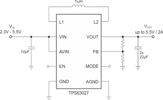
4 Typical Application
sp

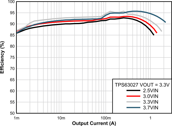
Efficiency vs Output Current
