SLVSC58B June 2016 – March 2019 TPS63070
PRODUCTION DATA.
- 1 Features
- 2 Applications
- 3 Description
- 4 Revision History
- 5 Device Comparison Table
- 6 Pin Configuration and Functions
- 7 Specifications
- 8 Detailed Description
- 9 Application and Implementation
- 10Power Supply Recommendations
- 11Layout
- 12Device and Documentation Support
- 13Mechanical, Packaging, and Orderable Information
Package Options
Mechanical Data (Package|Pins)
- RNM|15
Thermal pad, mechanical data (Package|Pins)
Orderable Information
8.5.1 Power Save Mode
Depending on the load current, in order to provide the best efficiency over the complete load range, the device works in PWM mode at an inductor current of approximately 650 mA or higher. At lighter load, the device switches automatically in to Power Save Mode to reduce power consumption and extend battery life. The PFM/PWM pin can be used to select between the two different operation modes. To enable Power Save Mode, the PFM/PWM pin must be set high.
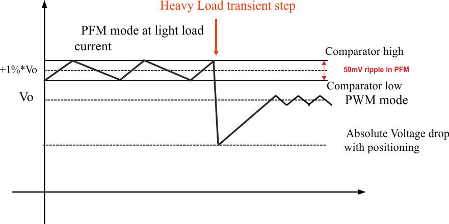
During Power Save Mode, the part operates with a reduced switching frequency and supply current to maintain high efficiency. The output voltage is monitored by a comparator for the threshold "comp low" and "comp high" at every clock cycle. When the device enters Power Save Mode, the converter stops operating and the output voltage drops. The slope of the output voltage depends on the load and the output capacitance. When the output voltage reaches the comp low threshold, at the next clock cycle the device ramps up the output voltage again by starting operation. Operation can last for one or several pulses until the "comp high" threshold is reached. At the next PFM cycle, if the inductor current is still lower than about 650 mA, the device switches off again and the same operation is repeated. Instead, if at the next PFM cycle, the inductor current is above approximately 650 mA , the device automatically switches to PWM mode.
In order to keep high efficiency in PFM mode, there is only a comparator active to keep the output voltage regulated. The AC ripple in this condition is increased, compared to the voltage in PWM mode. The amplitude of this voltage ripple typically is 50 mV pk-pk, with 22 µF effective capacitance. In order to avoid a critical voltage drop when switching from 0 A to full load, the output voltage in PFM is typically 1 % above the nominal value in PWM. This allows the converter to operate with a small output capacitor and still have a low absolute voltage drop during heavy load transients.
Power Save Mode can be disabled by programming the PFM/PWM pin low.
 Figure 9. Dynamic Voltage Positioning