SLVSEU9D November 2018 – January 2021 TPS63802
PRODUCTION DATA
- 1 Features
- 2 Applications
- 3 Description
- 4 Revision History
- 5 Description (continued)
- 6 Device Comparison Table
- 7 Pin Configuration and Functions
- 8 Specifications
-
9 Detailed Description
- 9.1 Overview
- 9.2 Functional Block Diagram
- 9.3
Feature Description
- 9.3.1 Control Loop Description
- 9.3.2 Precise Device Enable: Threshold- or Delayed Enable
- 9.3.3 Mode Selection (PFM/PWM)
- 9.3.4 Undervoltage Lockout (UVLO)
- 9.3.5 Soft Start
- 9.3.6 Adjustable Output Voltage
- 9.3.7 Overtemperature Protection - Thermal Shutdown
- 9.3.8 Input Overvoltage - Reverse-Boost Protection (IVP)
- 9.3.9 Output Overvoltage Protection (OVP)
- 9.3.10 Power-Good Indicator
- 9.4 Device Functional Modes
- 10Application and Implementation
- 11Power Supply Recommendations
- 12Layout
- 13Device and Documentation Support
- 14Mechanical, Packaging, and Orderable Information
Package Options
Mechanical Data (Package|Pins)
- DLA|10
Thermal pad, mechanical data (Package|Pins)
Orderable Information
3 Description
The TPS63802 is a high efficiency, high output current buck-boost converter. Depending on the input voltage, it automatically operates in boost, buck, or in a novel 4-cycle buck-boost mode when the input voltage is approximately equal to the output voltage. The transitions between modes happen at defined thresholds and avoid unwanted toggling within the modes to reduce output voltage ripple. The device output voltages are individually set by a resistive divider within a wide output voltage range. An 11-μA quiescent current enables the highest efficiency for little to no-load conditions.
| PART NUMBER | PACKAGE(1) | BODY SIZE (NOM) |
|---|---|---|
| TPS63802 | 10-Pin VSON-HR (0.5 mm pitch) | 3.0 mm × 2.0 mm |
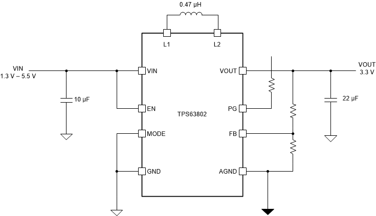
 Typical Application
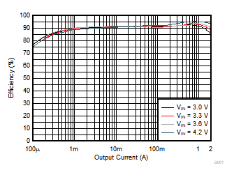
 Efficiency vs Output Current
(VO = 3.3 V)