SLVSC01A June 2013 – April 2015 TPS65133
PRODUCTION DATA.
- 1 Features
- 2 Applications
- 3 Description
- 4 Typical Application
- 5 Revision History
- 6 Pin Configuration and Functions
- 7 Specifications
- 8 Detailed Description
- 9 Application and Implementation
- 10Power Supply Recommendations
- 11Layout
- 12Device and Documentation Support
- 13Mechanical, Packaging, and Orderable Information
Package Options
Mechanical Data (Package|Pins)
- DPD|12
Thermal pad, mechanical data (Package|Pins)
- DPD|12
Orderable Information
9 Application and Implementation
NOTE
Information in the following applications sections is not part of the TI component specification, and TI does not warrant its accuracy or completeness. TI’s customers are responsible for determining suitability of components for their purposes. Customers should validate and test their design implementation to confirm system functionality.
9.1 Application Information
The TPS65133 device can be used to generate ±5-V supply rails from input supply voltages in the range 2.9 V to 5 V, and has been optimized for use with regulated 3.3-V rails and single-cell Li-Ion batteries. Its output voltages are fixed at ±5 V and cannot be changed by the user. Both output voltages are controlled by the EN pin: a high logic level on the EN pin enables both outputs, and a low logic level disables them. Note that when the input supply voltage is above the UVLO threshold and the EN pin is low, both outputs are disabled and actively discharged to ground. When the input supply voltage is below the UVLO threshold, both outputs are disabled, but they are not actively discharged.
9.2 Typical Application
Figure 9 shows a typical application schematic suitable for supplying up to 250 mA at ±5 V from e.g. a single-cell Li-Ion battery.
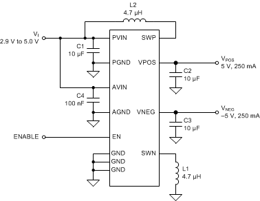 Figure 9. Typical Application Circuit
9.2.1 Design Requirements
The design parameters for the application circuit in Figure 9 are listed in Table 1.
Table 1. Design Parameters
| PARAMETERS | EXAMPLE VALUES |
|---|---|
| Input voltage range | 2.9 V to 5.0 V |
| Output voltage | ±5.0 V |
| Switching frequency | 1.7 MHz |
9.2.2 Detailed Design Procedure
In order to maximize performance, the TPS65133 device has been optimized for use with a relatively narrow range of external components, and customers are recommended to use the application circuit shown in Figure 9 and the components listed in Table 2 and Table 3.
9.2.2.1 Inductor Selection
The two dc-dc converters in the TPS65133 device have been optimized for use with 4.7 µH inductors, and it is recommended to use this value in all applications. Customers using different values of inductors should characterize performance thoroughly before going to mass production.
Table 2. Inductor Selection
| PARAMETER | VALUE | MANUFACTURER | PART NUMBER |
|---|---|---|---|
| L1, L2 | 4.7 µH | Coilmaster | MMPP252012-4R7N |
| Toko | 1239AS-H-4R7M | ||
| ABCO | LPP252012-4R7N | ||
| Coilcraft | XFL4020-4R7ML |
9.2.2.2 Capacitor Selection
The recommended capacitor values are shown in Table 3. Applications using less than the recommended capacitance (e.g. to save PCB area) may experience increased voltage ripple. In general, the lower the output power required by the application, the lower the capacitance needed for proper performance. C4 improves immunity to noise on the input supply voltage, but it is not necessary in many applications.
Table 3. Capacitor Selection
| PARAMETER | VALUE | MANUFACTURER | PART NUMBER |
|---|---|---|---|
| C1, C2, C3 | 10 µF | Murata | GRM21BR71A106KE51 |
| C4 | 100 nF | GRM21BR71E104KA01 |
9.2.3 Application Performance Graphs
The performance shown in the following graphs was obtained using the circuit shown in Figure 9 and the external components listed in Table 2 and Table 3.
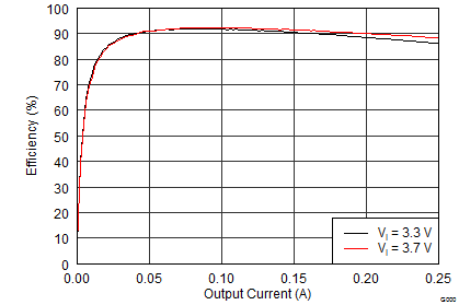
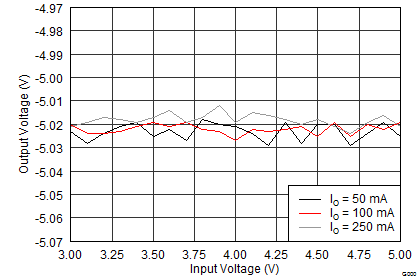
| VI = 3.7 V | ||
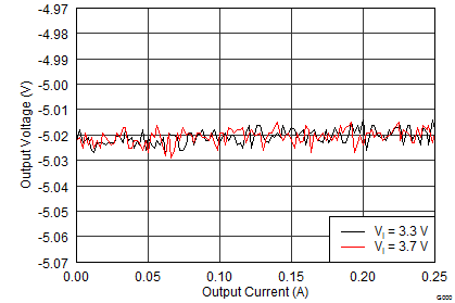
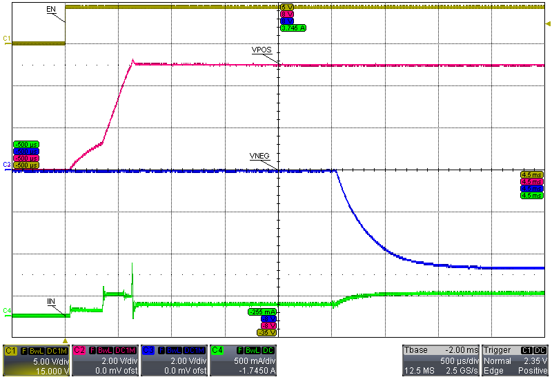
| VI = 3.7 V, IPOS = INEG = 100 mA | ||
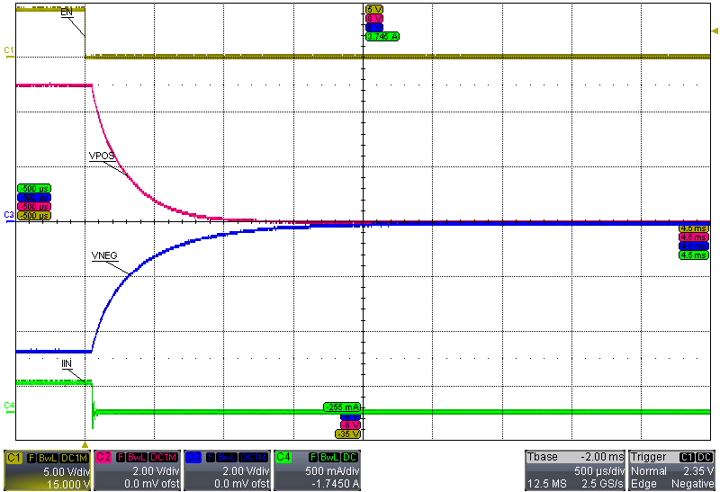
| VI = 3.7 V, IPOS = INEG = 100 mA | ||
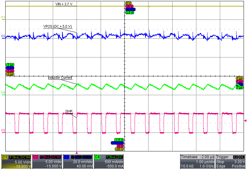
| VI = 3.7 V, IPOS = 100 mA | ||
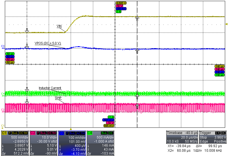
| VI = 3.7 V to 4.2 V, IPOS = 50 mA | ||
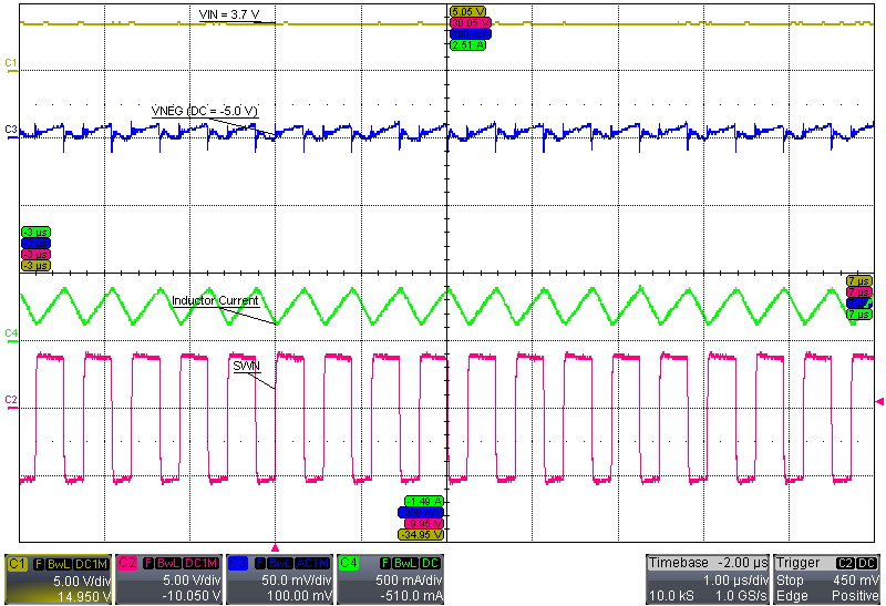
| VI = 3.7 V, INEG = 100 mA | ||
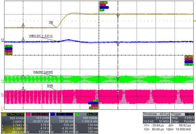
| VI = 3.7 V to 4.2 V, INEG = 50 mA | ||
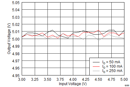
| VI = 3.7 V | ||
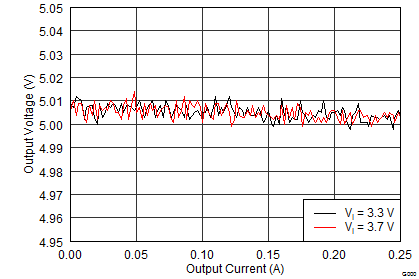
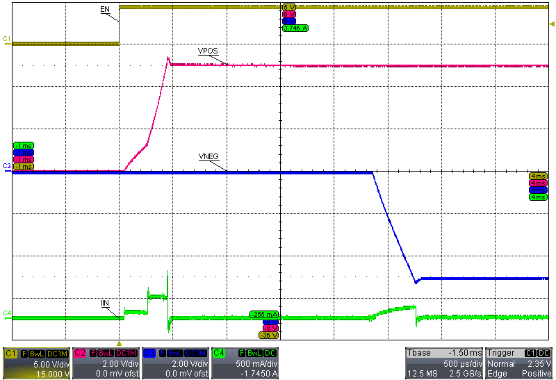
| VI = 3.7 V, IPOS = INEG = 0 mA | ||
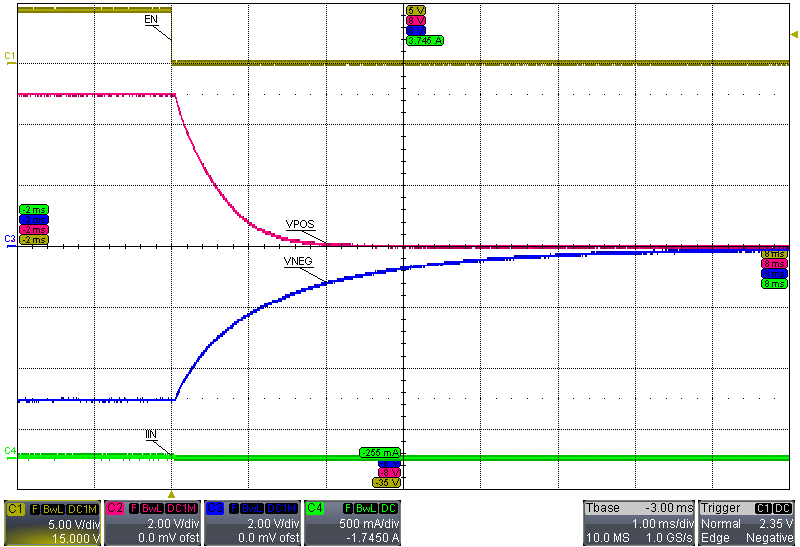
| VI = 3.7 V, IPOS = INEG = 0 mA | ||
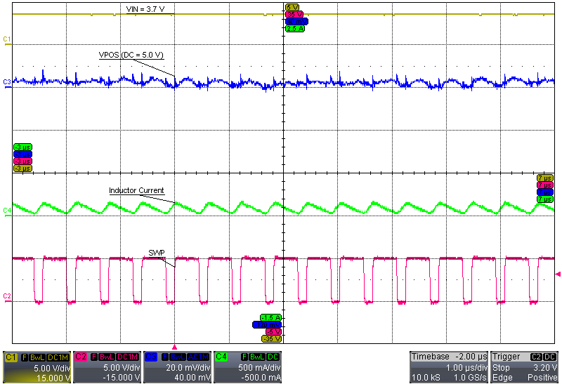
| VI = 3.7 V, IPOS = 10 mA | ||
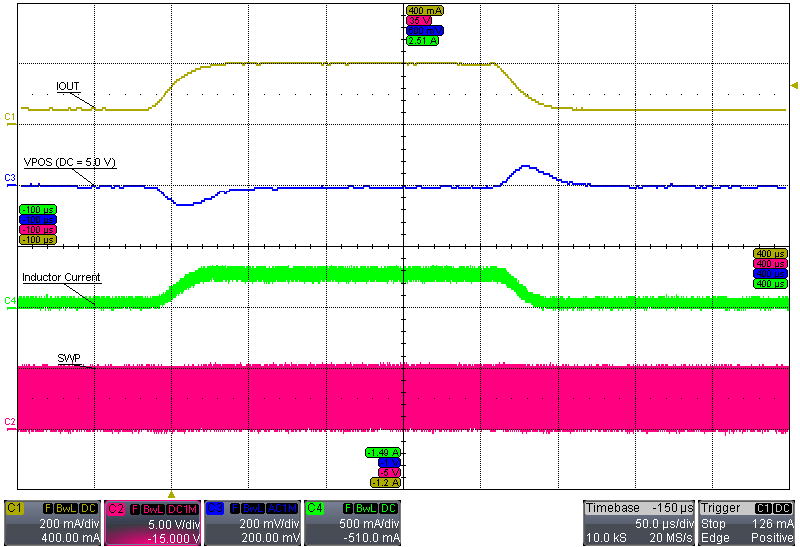
| VI = 3.7 V, IPOS = 50 mA to 200 mA | ||
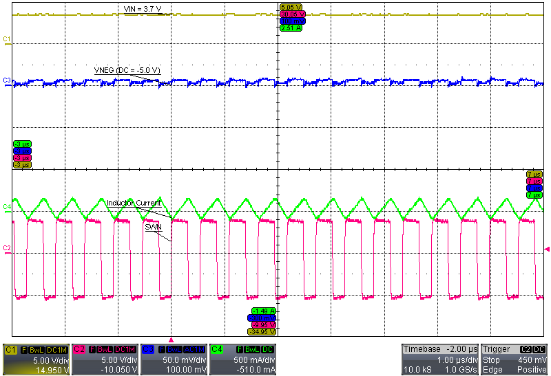
| VI = 3.7 V, INEG = 10 mA | ||
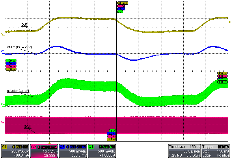
| VI = 3.7 V, INEG = 50 mA to 200 mA | ||
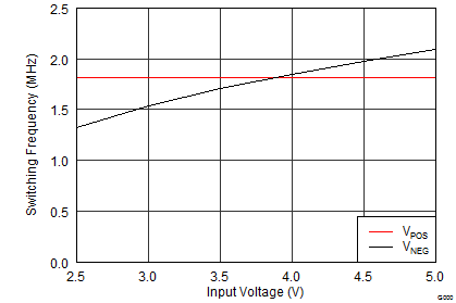
| IPOS = INEG = 100 mA | ||