SLVSA76G March 2010 – January 2016 TPS65180B , TPS65181 , TPS65181B
PRODUCTION DATA.
- 1 Features
- 2 Applications
- 3 Description
- 4 Revision History
- 5 Description (continued)
- 6 Device Comparison Table
- 7 Pin Configuration and Functions
- 8 Specifications
-
9 Detailed Description
- 9.1 Overview
- 9.2 Functional Block Diagram
- 9.3 Feature Description
- 9.4 Device Functional Modes
- 9.5
Register Maps
- 9.5.1 Thermistor Readout (TMST_VALUE) Register (Offset = 0x00h)
- 9.5.2 Enable (ENABLE) Register (Offset = 0x01h)
- 9.5.3 Positive Voltage Rail Adjustment (VP_ADJUST) Register (Offset = 0x02h)
- 9.5.4 Negative Voltage Rail Adjustment (VN_ADJUST) Register (Offset = 0x03h)
- 9.5.5 VCOM Adjustment (VCOM_ADJUST) Register (Offset = 0x04h)
- 9.5.6 Interrupt Enable 1 (INT_ENABLE1) Register (Offset = 0x05h)
- 9.5.7 Interrupt Enable 2 (INT_ENABLE2) Register (Offset = 0x06h)
- 9.5.8 Interrupt INT_STATUS1 (INT_STATUS1) Register (Offset = 0x07h)
- 9.5.9 Interrupt Status 2 (INT_STATUS2) Register (Offset = 0x08h)
- 9.5.10 Power Sequence Register 0 (PWR_SEQ0) Register (Offset = 0x09h)
- 9.5.11 Power Sequence Register 1 (PWR_SEQ1) Register (Offset = 0x0Ah)
- 9.5.12 Power Sequence Register 2 (PWR_SEQ2) Register (Offset = 0x0Bh)
- 9.5.13 Thermistor Configuration Register (TMST_CONFIG) (Offset = 0x0Ch)
- 9.5.14 Thermistor Hot Threshold (TMST_OS) Register (Offset = 0x0Dh)
- 9.5.15 Thermistor Cool Threshold (TMST_HYST) Register (Offset = 0x0Eh)
- 9.5.16 Power-Good Status (PG_STATUS) Register (Offset = 0x0Fh)
- 9.5.17 Revision and Version Control (REVID) Register (Offset = 0x10h)
- 9.5.18 I2C Read Pointer Control (FIX_READ_POINTER) Register (Offset = 0x11h) (TPS65181 and TPS65181B ONLY)
-
10Application and Implementation
- 10.1
Application Information
- 10.1.1 Dependencies Between Rails
- 10.1.2 Soft-Start
- 10.1.3 VCOM Adjustment
- 10.1.4 VCOM Adjustment Through Register Control
- 10.1.5 VCOM Adjustment Through External Potentiometer
- 10.1.6 VPOS and VNEG Supply Tracking
- 10.1.7 Fault Handling and Recovery
- 10.1.8 TPS65180 and TPS65180B Fault Handling
- 10.1.9 TPS65181 and TPS65181B Fault Handling
- 10.1.10 Power-Good Pin
- 10.1.11 Interrupt Pin
- 10.1.12 Panel Temperature Monitoring
- 10.1.13 NTC Bias Circuit
- 10.1.14 TPS65180 and TPS65180B Temperature Acquisition
- 10.1.15 TPS65181 and TPS65181B Temperature Acquisition
- 10.1.16 Overtemperature Reporting
- 10.1.17 Overtemperature Fault Queuing
- 10.1.18 TPS65181 and TPS65181B Temperature Sensor
- 10.1.19 I2C Bus Operation
- 10.2 Typical Application
- 10.1
Application Information
- 11Power Supply Recommendations
- 12Layout
- 13Device and Documentation Support
- 14Mechanical, Packaging, and Orderable Information
Package Options
Mechanical Data (Package|Pins)
- RGZ|48
Thermal pad, mechanical data (Package|Pins)
- RGZ|48
Orderable Information
10 Application and Implementation
NOTE
Information in the following applications sections is not part of the TI component specification, and TI does not warrant its accuracy or completeness. TI’s customers are responsible for determining suitability of components for their purposes. Customers should validate and test their design implementation to confirm system functionality.
10.1 Application Information
10.1.1 Dependencies Between Rails
Charge pumps, LDOs, and VCOM driver are dependent on the positive and inverting buck-boost converters and several dependencies exist that affect the power-up sequencing. These dependencies are listed as follows:
- Inverting buck-boost (DCDC2) must be in regulation before positive boost (DCDC1) can be enabled. Internally, DCDC1 enable is gated by DCDC2 power-good.
- Positive boost (DCDC1) must be in regulation before LDO2 (VNEG) can be enabled. Internally LDO2 enable is gated DCDC1 power-good.
- Positive boost (DCDC1) must be in regulation before VCOM can be enabled; Internally VCOM enable is gated by DCDC1 power-good.
- Positive boost (DCDC1) must be in regulation before negative charge pump (CP2) can be enabled. Internally CP2 enable is gated by DCDC1 power-good.
- Positive boost (DCDC1) must be in regulation before positive charge pump (CP1) can be enabled. Internally CP1 enable is gated by DCDC1 power-good.
- LDO2 must be in regulation before LDO1 can be enabled. Internally LDO1 enable is gated by LDO2 power-good.
- The minimum delay time between any two PWRx pins must be > 62.5 µs in order to follow the power up sequence defined by GPIO control. If any two PWRx pins are pulled up together (< 62.5 µs apart) or the sequencer tries to bring up the rails at the same time by assigning the same STROBE to rails in PWR_SEQ0 register, rails is staggered in a manner that an enable od the subsequent rail is gated by PG of a preceding rail. In this case, the default order of power-up is LDO2 (VNEG), CP2 (VEE), LDO1 (VPOS), and CP1(VDDH). If any two PWRx pins are pulled low together or the sequencer tries to bring down the rails at the same time by assigning the same STROBE to rails in PWR_SEQ0 register, then all rails goes down at the same time.
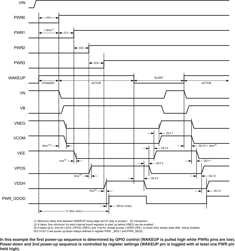 Figure 5. Power-Up and Power-Down Timing Diagram
10.1.2 Soft-Start
Soft-start for DCDC1, DCDC2, LDO1, and LDO2 is accomplished by lowering the current limits during start-up. If DCDC1 or DCDC2 are unable to reach power-good status within 10 ms, the corresponding UV flag is set in the interrupt registers, the interrupt pin is pulled low, and the device enters STANDBY mode. LDO1, LDO2, positive and negative charge pumps have a 5-ms power-good timeout limit. If either rail is unable to power up within 5 ms after it has been enabled, the corresponding UV flag is set and the interrupt pin is pulled low. However, the device remains in ACTIVE mode in this case.
10.1.3 VCOM Adjustment
Through the I2C interface the user can select between two methods of VCOM voltage adjustment:
- Using the internal 8-bit DAC and register control.
- Using an external voltage source (resistor divider) connected to the VCOM_XADJ pin.
10.1.4 VCOM Adjustment Through Register Control
By default the TPS65180x is setup for internal VCOM control through the I2C interface. The default setting for the 8-bit DAC is 0x74h which results in 1.25 V ±0.8% for VCOM. VCOM can be adjusted up or down in steps of
11 mV (typical) by writing to the VCOM_ADJUST register. The output range for VCOM is limited to –0.3 V to –2.5 V.
 Figure 6. Block Diagram of VCOM Circuit
10.1.5 VCOM Adjustment Through External Potentiometer
VCOM can be adjusted by an external potentiometer by setting the VCOM_ADJ bit of the VN_ADJUST register to 0 and connecting a potentiometer to the VCOM_XADJ pin. The potentiometer must be connected between ground and a negative supply as shown in Figure 6. The gain from VCOM_XADJ to VCOM is 1 and therefore the voltage applied to VCOM_XADJ pin must range from –0.3 V to –2.5 V.
10.1.6 VPOS and VNEG Supply Tracking
LDO1 (VPOS) and LDO2 (VNEG) track each other in a way that they are of opposite sign but same magnitude. The sum of VLDO1 and VLOD2 is guaranteed to be < 50 mV. To ensure proper tracking of the supplies the VPOS_SET[2:0] bits of the VP_ADUST register must remain at the default setting of 010b. To adjust the VPOS and VNEG output voltage, write to the VN_ADJUST register only and keep the VPOS_SET[2:0] bits of the VP_ADUST register unchanged.
10.1.7 Fault Handling and Recovery
The TPS6518x and TPS65181xB monitor input and output voltages and die temperature and takes action if operating conditions are outside normal limits. Whenever the TPS6518x and TPS65181xB encounter:
- Thermal shutdown (TSD)
- Positive boost undervoltage (VB_UV)
- Inverting buck-boost undervoltage (VN_UV)
- Input undervoltage lockout (UVLO)
it shuts down all power rails and enter STANDBY mode. Shutdown follows the reverse power-up sequence defined by the PWR_SEQx registers. When a fault is detected, the PWR_GOOD and nINT pin are pulled low and the corresponding interrupt bit is set in the interrupt register.
Whenever the TPS6518x and TPS65181xB encounter undervoltage on VNEG (VNEG_UV), VPOS (VPOS_UV), VEE (VEE_UV) or VDDH (VDDH_UV) it shuts down the corresponding rail (plus any dependent rail) only and remain in ACTIVE mode, allowing the DCDC converters to remain up. Again, the PWR_GOOD and nINT pins is pulled low and the corresponding interrupt bit is set.
10.1.8 TPS65180 and TPS65180B Fault Handling
When a fault is detected, the TPS65180 and TPS65180B set the appropriate interrupt flags in the INT_STATUS1 and INT_STATUS2 registers and pull the INT pin low to signal an interrupt to the host processor. None of the power rails can be re-enabled before the host has read the INT_STATUSx bits and the fault has been removed. As the PWRx inputs are edge-sensitive, the host must also toggle the PWRx pins to re-enable the rails through GPIO control, that is, it must bring the PWRx pins low before asserting them again.
10.1.9 TPS65181 and TPS65181B Fault Handling
The TPS65181 and TPS65181 do not require the host processor to access the INT_STATUS registers before re-enabling the output rails. Rails can be re-enabled as soon as the fault condition has been removed. Again, as the PWRx inputs are edge-sensitive, the host must also toggle the PWRx pins to re-enable the rails through GPIO control, that is, it must bring the PWRx pins low before asserting them again.
10.1.10 Power-Good Pin
The power-good pin (PWR_GOOD) is an open-drain output that is pulled high when all four power rails (CP1, CP2, LDO1, LDO2) are in regulation and is pulled low if any of the rails encounters a fault. PWR_GOOD remains low if one of the rails is not enabled by the host and only after all rails are in regulation PWR_GOOD is released to Hi-Z state (pulled up by external resistor).
10.1.11 Interrupt Pin
The interrupt pin (nINT) is an open-drain output that is pulled low whenever one or more of the INT_STATUS1 or INT_STATUS2 bits are set. The nINT pin is released (returns to Hi-Z state) and fault bits are cleared when the register with the set bit has been read by the host. If the fault persists, the INT_pin is pulled low again after a maximum of 32 µs.
Interrupt events can be masked by re-setting the corresponding enable bit in the INT_ENABLE1 and INT_ENABLE2 register, that is, the user can determine which events cause the nINT pin to be pulled low. The status of the enable bits affects the nINT pin only and has no effect on any of the protection and monitoring circuits or the INT_STATUSx bits themselves.
Note that persisting fault conditions such as thermal shutdown can cause the nINT pin to be pulled low for an extended period of time which can keep the host in a loop trying to resolve the interrupt. If this behavior is not desired, set the corresponding mask bit after receiving the interrupt and keep polling the INT_STATUSx register to see when the fault condition has disappeared. After the fault is resolved, unmask the interrupt bit again.
10.1.12 Panel Temperature Monitoring
The TPS6518x and TPS65181xB provide circuitry to bias and measure an external negative temperature coefficient resistor (NTC) to monitor device temperature in a range from –10°C to 85°C with and accuracy of ±1°C from 0°C to 50°C. The TPS65180 and TPS65180B require the host to trigger the temperature acquisition through an I2C command whereas the TPS65181 and TPS65181B trigger the temperature acquisition automatically once every 60 s.
10.1.13 NTC Bias Circuit
Figure 7 below shows the block diagram of the NTC bias and measurement circuit. The NTC is biased from an internally generated 2.25-V reference voltage through an integrated 7.307-kΩ bias resistor. A 43-kΩ resistor is connected parallel to the NTC to linearize the temperature response curve. The circuit is designed to work with a nominal 10-kΩ NTC and achieves accuracy of ±1°C from 0°C to 50°C. The voltage drop across the NTC is digitized by a 10-bit SAR ADC and translated into an 8-bit two’s complement by digital per Table 2.
Table 2. ADC Output Value vs Termperature
| TEMPERATURE | TMST_VALUE[7:0] |
|---|---|
| < –10°C | 1111 0110 |
| –10°C | 1111 0110 |
| –9°C | 1111 0111 |
| ... | ... |
| –2°C | 1111 1110 |
| –1°C | 1111 1111 |
| 0°C | 0000 0000 |
| 1°C | 0000 0001 |
| 2°C | 0000 0010 |
| ... | ... |
| 25°C | 0001 1001 |
| ... | |
| 85°C | 0101 0101 |
| > 85°C | 0101 0101 |
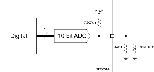 Figure 7. NTC Bias and Measurement Circuit
10.1.14 TPS65180 and TPS65180B Temperature Acquisition
The TPS65180 and TPS65180B require the host to trigger the temperature acquisition before reading the temperature value from register TMST_VALUE. A standard temperature measurement involves the following steps:
- The host sets the READ_THERM bit of the TMST_CONFIG register to 1. This enabled the NTC bias circuit and internal ADC.
- The analog to digital conversion is automatically started after a fixed 250-µs delay. While the conversion is in progress the CONV_END bit of the TMST_CONFIG register is held low and returns to 1 after the conversion result is available.
- After the conversion is complete the READ_THERM bit is automatically reset, the EOC bit of the INT_STATUS2 register is set, and the interrupt pin (nINT) is pulled low.
- The host services the interrupt by reading the INT_STATUS2 register. This clears the interrupt pin (nINT pin returns high). The host sees the EOC bit set and knows that the temperature data is available in the TMST_VALUE register.
- The host reads the temperature data from the TMST_VALUE register.
10.1.15 TPS65181 and TPS65181B Temperature Acquisition
The TPS65181 and TPS65181B trigger temperature acquisition once every 60s to reduce the number of required I2C writes. The host or display timing controller can read the temperature at any time by accessing the TMST_VALUE register without having to set the READ_THERM bit first. However, the host can always trigger an additional temperature reading the same way as for the TPS65180 and TPS65180B.
NOTE
At the end of each temperature acquisition, the EOC interrupt is set and an interrupt is issued. Although the interrupt is automatically cleared, the nINT pin is pulled low for a short amount of time (6 µs). To avoid seeing the EOS interrupt every 60s, TI recommends to mask the EOC interrupt by setting the EOC_EN bit of the INT_ENABLE2 register to 0.
10.1.16 Overtemperature Reporting
The user has the option of setting HOT and COOL (not HOT) temperature thresholds as well as controlling interrupt behavior as the NTC exceeds HOT and cools down below COOL (not-HOT) threshold.
By default, TPS6518x and TPS65181xB compare the temperature conversion result to the HOT threshold after each conversion. If the NTC temperature is above the HOT threshold, the TMST_HOT bit in the INT_STATUS1 register is set to 1 and the interrupt pin (nINT) is pulled low. HOT temperature threshold is set by the host by writing to the TMST_OS register and the HOT interrupt can be disabled by setting the HOT_EN bit of the INT_ENABLE1 register to 0.
When the device has detected that the NTC is above the HOT threshold it compares subsequent temperature acquisitions against the COOL threshold and pull the interrupt pin low when the NTC temperature drops below the COOL threshold. However, the interrupt is issued only if the host has unmasked the COOL interrupt by setting TMST_COOL_EN bit of INT_ENABLE1 register to 1. The COOL threshold is set by the host by writing to the TMST_HYST register.
To use the full functionality of the HOT/COOL interrupts the following actions are required:
- The host sets the HOT and COOL (not HOT) thresholds by writing the TMST_OS and TMST_HYST registers.
- (2) For TPS65180 and TPS65180B only: The host sets the READ_THERM bit of the TMST_CONFIG register to 1. This initiates the temperature acquisition.
- TPS6518x and TPS65181xB compare the result against the TMST_OS threshold and pulls the nINT pin low if the NTC temperature exceeds the HOT threshold.
- If the TPS6518x and TPS65181xB report a HOT condition, the host unmasks the TMST_COOL_EN bit by setting it to 1 (INT_ENABLE1 register).
- The host initiates a new temperature conversion by setting the READ_THERM bit of the TMST_CONFIG register to 1. If the new temperature is still above the HOT threshold, a new HOT interrupt is issued. If the temperature is below HOT but above COOL threshold, no interrupt is issued (except for EOC which is issued at the end of each conversion). If the temperature is below COOL threshold, a COOL interrupt is issued.
- After the temperature drops below the COOL threshold the host must set the TMST_COOL_EN bit in the INT_ENABLE1 register to 0 to mask additional COOL interrupts after subsequent temperature acquisitions.
10.1.17 Overtemperature Fault Queuing
The user can specify the number of consecutive HOT temperature reads required to issue a HOT interrupt. The user can set the FAULT_QUE[1:0] bits of the TMST_CONFIG register to specify 1, 2, 4, or 6 consecutive reads that all must be above the HOT threshold before a HOT interrupt is issued. The fault queue is reset each time the acquired temperature drops below the HOT threshold and can also be reset by the host by setting the FAULT_QUE_CLR bit 1. Only if the specified number of readings have been detected which all need to be above the HOT threshold, a HOT interrupt is issued. This function is useful to reduce noise in the temperature measurements.
10.1.18 TPS65181 and TPS65181B Temperature Sensor
The TPS65181 and TPS65181B automates the temperature monitoring process and is specifically designed to operate in multi-host systems where one of the I2C hosts, for eaxmple, the display controller, has limited I2C capability. Standard I2C protocol requires the following steps to read data from a register:
- Send device and register address, R/nW bit set low (write command).
- Send device address, R/nW set high (read command).
- The slave responds with data from the specified register address.
Some display controllers support I2C read commands only and need to access the temperature data from the TPS65181 and TPS65181B TMST_VALUE register. To support these systems the TPS65181 and TPS65181B automatically trigger temperature acquisition every 60s (for other acquisition intervals contact the factory) and stores the result in TMST_VALUE register. With the FIX_RD_PTR bit in the FIX_RD_POINTER register set to 1 the device responds to any I2C read command with data from the TMST_VALUE register. No write command with the register address is required and address auto increment feature is disabled in this mode. Therefore reading the temperature data is reduced to two steps:
- Send device address, R/nW set high (read command).
- Read the data from the slave. The slave responds with data from TMST_VALUE register address.
Write functionality is not affected by the FIX_RD_PTR bit and the main controller in the system maintains full control of the PMIC. Interrupts and error flags are issued and need to be handled the same way as for the TPS65180 and TPS65180B with two exceptions:
- The FIX_RD_PTR bit in the FIX_RD_POINTER register needs to be set to 0 before the main controller can read any register different from the TMST_VALUE register.
- Thermal shutdown (TSD), positive boost undervoltage (VB_UV), inverting buck-boost undervoltage (VN_UV), and input undervoltage lockout (UVLO) interrupt bits do not have to be cleared before output rails can be re-enabled.
At system power-up the main processor sets up the PMIC by accessing the I2C registers and setting the control parameters as needed. When the system is set up correctly, the main controller sets the FIX_READ_POINTER bit and the display controller can start accessing the temperature information. During normal operation the main controller can write to the PMIC at any time but before it can read access registers the FIX_READ_POINTER bit must be written 0.
The temperature range and representation of the temperature data is the same between the TPS65180 and TPS65180B or the TPS65181 and TPS65181B.
10.1.19 I2C Bus Operation
The TPS6518x and TPS65181xB host a slave I2C interface that supports data rates up to 400 kbps and auto-increment addressing and is compliant to I2C standard 3.0.
 Figure 8. Subaddress in I2C Transmission
| Start – Start condition | ACK – Acknowledge |
| G(3:0) – Group ID: Address fixed at 1001. | S(7:0) – Subaddress: defined per register map. |
| A(2:0) – Device Address: Address fixed at 000. | D(7:0) – Data; Data to be loaded into the device. |
| R/nW – Read / not Write Select Bit | Stop – Stop condition |
The I2C Bus is a communications link between a controller and a series of slave terminals. The link is established using a two-wired bus consisting of a serial clock signal (SCL) and a serial data signal (SDA). The serial clock is sourced from the controller in all cases where the serial data line is bidirectional for data communication between the controller and the slave terminals. Each device has an open-drain output to transmit data on the serial data line. An external pullup resistor must be placed on the serial data line to pull the drain output high during data transmission.
Data transmission is initiated with a start bit from the controller as shown in Figure 10. The start condition is recognized when the SDA line transitions from high to low during the high portion of the SCL signal. Upon reception of a start bit, the device receives serial data on the SDA input and check for valid address and control information. If the appropriate group and address bits are set for the device, then the device issues an acknowledge pulse and prepare the receive subaddress data. Subaddress data is decoded and responded to as per the Register Maps section of this document. Data transmission is completed by either the reception of a stop condition or the reception of the data word sent to the device. A stop condition is recognized as a low to high transition of the SDA input during the high portion of the SCL signal. All other transitions of the SDA line must occur during the low portion of the SCL signal. An acknowledge is issued after the reception of valid address, sub-address and data words. The I2C interface auto-sequences through register addresses, so that multiple data words can be sent for a given I2C transmission. Reference Figure 10.
NOTE
Auto-increment is not supported when the FIX_RD_PTR bit is set (TPS65181/TPS65181B only).

Bottom: I2C READ data transmission with FIX_RD_PTR bit set for EPSON Broadsheet support.
Only address 0x00h can be read. FIX_RD_PTR bit has no impact on WRITE transaction.
 Figure 10. I2C Start, Stop, and Acknowledge Protocol
 Figure 11. I2C Data Transmission Timing
10.2 Typical Application
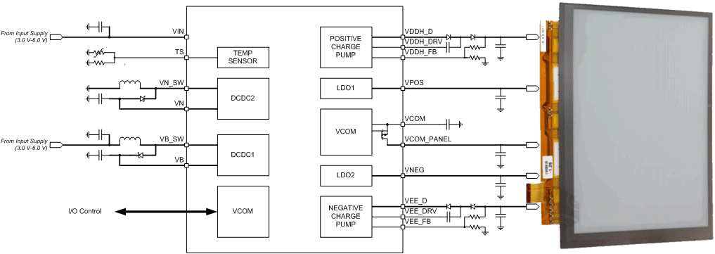 Figure 12. Typical Application
10.2.1 Design Requirements
For this design example, use the parameters listed in Table 3.
Table 3. Design Parameters
| VOLTAGE | SEQUENCE (STROBE) | |
|---|---|---|
| VNEG (LDO2) | –15 V | 1 |
| VEE (Charge pump 2) | –20 V | 2 |
| VPOS (LDO1) | 15 V | 3 |
| VDDH (charge pump 1) | 22 V | 4 |
10.2.2 Detailed Design Procedure
For the positive boost regulator (DCDC1) a 10-µF capacitor can be used as the input capacitor value; two 4.7-µF capacitor are used as output capacitors to reduce ESR along with a 2.2-µH inductor. For the inverting buck-boost regulator (DCDC2) an 10-µF capacitor can be used at the input capacitor value; A 10-µF and 4.7-µF capacitor are used as output capacitors to reduce ESR, with a 4.7-µH inductor. Capacitor ESR for all capacitors should be around 20 mΩ, and ceramic X5R material. These are the typical the values used, additional inductor and capacitor values can be used for improved functionality, but the parts should be rated the same as the recommended external components listed in Table 4.
Table 4. Recommended External Components
| PART NUMBER | VALUE | SIZE | MANUFACTURER | |
|---|---|---|---|---|
| INDUCTORS | ||||
| LQH44PN4R7MP0 | 4.7 µH | 4.00 mm × 4.00 mm × 1.65 mm | Murata | |
| VLS252012T-2R2M1R3 | 2.2 µH | 2.00 mm × 2.50 mm × 1.20 mm | TDK | |
| CAPACITORS | ||||
| GRM21BC81E475KA12L | 4.7-µF, 25-V, X6S | 805 | Murata | |
| GRM32ER71H475KA88L | 4.7-µF, 50-V, X7R | 1210 | Murata | |
| All other caps | X5R or better | |||
| DIODES | ||||
| BAS3010 | SOD-323 | Infineon | ||
| MBR130T1 | SOD-123 | ON-Semi | ||
| THERMISTOR | ||||
| NCP18XH103F03RB | 10 kΩ | 603 | Murata | |
10.2.3 Application Curves
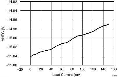 Figure 13. Load Current vs VNEG
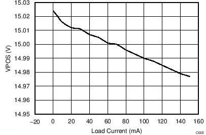 Figure 15. Load Current vs VPOS
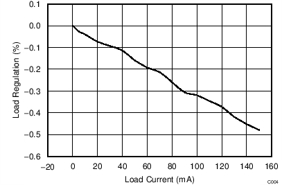 Figure 14. Load Current vs Load Regulation
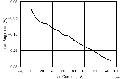 Figure 16. Load Current vs Load Regulation