SLVSDY9A March 2017 – November 2022 TPS65263-1Q1
PRODUCTION DATA
- 1 Features
- 2 Applications
- 3 Description
- 4 Revision History
- 5 Pin Configuration and Functions
- 6 Specifications
-
7 Detailed Description
- 7.1 Overview
- 7.2 Functional Block Diagram
- 7.3
Feature Description
- 7.3.1 Adjusting the Output Voltage
- 7.3.2 Enable and Adjusting UVLO
- 7.3.3 Soft-Start Time
- 7.3.4 Power-Up Sequencing
- 7.3.5 V7V Low-Dropout Regulator and Bootstrap
- 7.3.6 Out-of-Phase Operation
- 7.3.7 Output Overvoltage Protection (OVP)
- 7.3.8 PSM
- 7.3.9 Slope Compensation
- 7.3.10 Overcurrent Protection
- 7.3.11 Power Good
- 7.3.12 Thermal Shutdown
- 7.4 Device Functional Modes
- 7.5 Register Maps
- 8 Application and Implementation
- 9 Device and Documentation Support
- 10Mechanical, Packaging, and Orderable Information
Package Options
Mechanical Data (Package|Pins)
- RHB|32
Thermal pad, mechanical data (Package|Pins)
- RHB|32
Orderable Information
8.2.2.3 Input Capacitor Selection
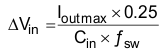
The TPS65263-1Q1 requires a high-quality ceramic, type X5R or X7R, input decoupling capacitor of at least 10 µF of effective capacitance on the PVIN input voltage pins. In some applications, additional bulk capacitance can also be required for the PVIN input. The effective capacitance includes any DC bias effects. The voltage rating of the input capacitor must be greater than the maximum input voltage. The capacitor must also have a ripple current rating greater than the maximum input current ripple of the TPS65263-1Q1. The input ripple current can be calculated using Equation 16.
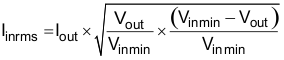
The value of a ceramic capacitor varies significantly over temperature and the amount of DC bias applied to the capacitor. The capacitance variations due to temperature can be minimized by selecting a dielectric material that is stable over temperature. X5R and X7R ceramic dielectrics are usually selected for power regulator capacitors because they have a high capacitance-to-volume ratio and are fairly stable over temperature. The output capacitor must also be selected with the DC bias taken into account. The capacitance value of a capacitor decreases as the DC bias across a capacitor increases. The input capacitance value determines the input ripple voltage of the regulator. Use Equation 17 to calculate the input voltage ripple.