SLVSCL3E June 2014 – May 2019 TPS65283 , TPS65283-1
PRODUCTION DATA.
- 1 Features
- 2 Applications
- 3 Description
- 4 Typical Schematic
- 5 Revision History
- 6 Description (continued)
- 7 Pin Configuration and Functions
- 8 Specifications
-
9 Detailed Description
- 9.1 Overview
- 9.2 Functional Block Diagram
- 9.3
Feature Description
- 9.3.1 Power Switch Detailed Description
- 9.3.2
Buck DC-DC Converter Detailed Description
- 9.3.2.1 Output Voltage
- 9.3.2.2 Adjustable Switching Frequency
- 9.3.2.3 Synchronization
- 9.3.2.4 Error Amplifier
- 9.3.2.5 Slope Compensation
- 9.3.2.6 Enable and Adjusting UVLO
- 9.3.2.7 Internal V7V Regulator
- 9.3.2.8 Short Circuit Protection
- 9.3.2.9 Bootstrap Voltage (BST) and Low Dropout Operation
- 9.3.2.10 Output Overvoltage Protection (OVP)
- 9.3.2.11 Power Good
- 9.3.2.12 Power-Up Sequencing
- 9.3.2.13 Thermal Performance
- 9.4 Device Functional Modes
- 10Application and Implementation
- 11Power Supply Recommendations
- 12Layout
- 13Device and Documentation Support
- 14Mechanical, Packaging, and Orderable Information
Package Options
Mechanical Data (Package|Pins)
- RGE|24
Thermal pad, mechanical data (Package|Pins)
- RGE|24
Orderable Information
9.3.2.12 Power-Up Sequencing
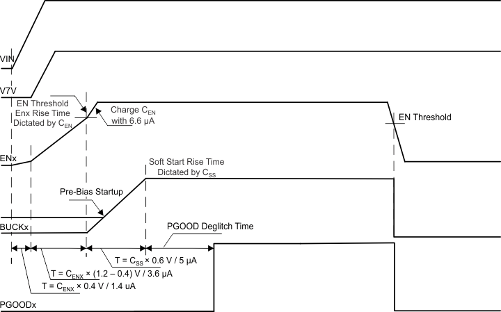
The TPS65283, TPS65283-1 has a dedicated enable pin for each converter. The converter enable pins are biased by a current source that allows for easy sequencing by the addition of an external capacitor. Disabling the converter with an active pulldown transistor on the ENx pin allows for predictable power-down timing operation. Figure 29 shows the timing diagram of a typical buck power-up sequence with connecting a capacitor at ENx pin.
A typical 1.4-µA current is charging ENx pin from input supply. When ENx pin voltage rise to typical 0.4 V, the internal V7V LDO turns on. A 3.6-µA pullup current is sourcing ENx. After ENx pin voltage reaches to ENx enabling threshold, 3-µA hysteresis current sources to the pin to improve noise sensitivity. The internal soft-start comparator compares internal SS voltage to 0.6 V, When internal SS voltage ramps up to 0.6 V, PGOODx monitor is enabled. After PGOODx deglitch time, and if output voltages are in the regulation, PGOODx is asserted.
 Figure 29. Start-Up Power Sequence