SLUSDU2A September   2019  – October 2020 TPS65296

PRODUCTION DATA  

  1. Features
  2. Applications
  3. Description
  4. Revision History
  5. Pin Configuration and Functions
  6. Specifications
    1. 6.1 Absolute Maximum Ratings
    2. 6.2 ESD Ratings
    3. 6.3 Recommended Operating Conditions
    4. 6.4 Thermal Information
    5. 6.5 Electrical Characteristics
    6. 6.6 Typical Characteristics
  7. Detailed Description
    1. 7.1 Overview
    2. 7.2 Functional Block Diagram
    3. 7.3 Feature Description
      1. 7.3.1 PWM Operation and D-CAP3 Control
      2. 7.3.2 Advanced Eco-mode Control
      3. 7.3.3 Soft Start and Prebiased Soft Start
      4. 7.3.4 Power Good
      5. 7.3.5 Overcurrent Protection and Undervoltage Protection
      6. 7.3.6 Overvoltage Protection
      7. 7.3.7 UVLO Protection
      8. 7.3.8 Output Voltage Discharge
      9. 7.3.9 Thermal Shutdown
    4. 7.4 Device Functional Modes
      1. 7.4.1 Light Load Operation for VDD1 Buck and VDD2 Buck
      2. 7.4.2 Output State Control
      3. 7.4.3 Output Sequence Control
  8. Application and Implementation
    1. 8.1 Application Information
    2. 8.2 Typical Application
      1. 8.2.1 Design Requirements
      2. 8.2.2 Detailed Design Procedure
        1. 8.2.2.1 External Component Selection
          1. 8.2.2.1.1 Inductor Selection
          2. 8.2.2.1.2 Output Capacitor Selection
          3. 8.2.2.1.3 Input Capacitor Selection
          4. 8.2.2.1.4 Bootstrap Capacitor and Resistor Selection
      3. 8.2.3 Application Curves
  9. Power Supply Recommendations
  10. 10Layout
    1. 10.1 Layout Guidelines
    2. 10.2 Layout Example
  11. 11Device and Documentation Support
    1. 11.1 Device Support
      1. 11.1.1 Third-Party Products Disclaimer
    2. 11.2 Support Resources
    3. 11.3 Receiving Notification of Documentation Updates
    4. 11.4 Trademarks
    5. 11.5 Electrostatic Discharge Caution
    6. 11.6 Glossary
  12. 12Mechanical, Packaging, and Orderable Information

Package Options

Mechanical Data (Package|Pins)
Thermal pad, mechanical data (Package|Pins)
Orderable Information

Description

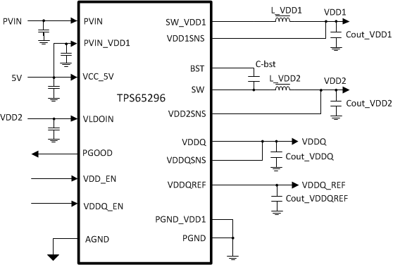
The TPS65296 device provides a complete power solution for LPDDR4/LPDDR4X memory system with the lowest total cost and minimum space. It meets the JEDEC standard for LPDDR4/LPDDR4X power-up and power-down sequence requirement. The TPS65296 integrates two synchronous buck converters (VDD1 and VDD2) and a 1.5-A LDO (VDDQ).

The TPS65296 employs D-CAP3™ mode with 600-kHz switching frequency for fast transient, good load/line regulation, and support for ceramic output capacitors without an external compensation circuit.

The TPS65296 provides rich functions as well as good efficiency with internal low Rdson power MOSFETs. It supports flexible power state control, placing VDDQ at high-Z in S3 and discharging VDD1, VDD2, and VDDQ in S4/S5 state. Full protection features include OVP, UVP, OCP, UVLO and thermal shutdown protection. The part is available in a thermally enhanced 18-pin HotRod™ VQFN package and is designed to operate under the –40°C to 125°C junction temperature range.

Device Information(1)
PART NUMBERPACKAGEBODY SIZE (NOM)
TPS65296VQFN (18)3.00 mm × 3.00 mm
For all available packages, see the orderable addendum at the end of the data sheet.
GUID-93F61AD6-F2B2-4D6A-ACAB-5BC74338EA20-low.gifTypical Application