SLVSCW2A September 2015 – February 2016 TPS657095
PRODUCTION DATA.
- 1 Features
- 2 Applications
- 3 Description
- 4 Revision History
- 5 Pin Configuration and Functions
- 6 Specifications
-
7 Detailed Description
- 7.1 Overview
- 7.2 Functional Block Diagram
- 7.3
Feature Description
- 7.3.1 State Diagram
- 7.3.2 Power-up Timing
- 7.3.3 GPO
- 7.3.4 GPIO
- 7.3.5 LED_EN
- 7.3.6 PWM Dimming
- 7.3.7 Crystal Oscillator and CLKOUT
- 7.3.8 LDOs
- 7.3.9 Undervoltage Lockout
- 7.3.10 Power Up/Power Down Default States
- 7.3.11 Output Voltage Discharge for LDO1 and LDO2
- 7.3.12 Power-Good Status Bits for LDO1 and LDO2
- 7.3.13 Short-Circuit Protection
- 7.3.14 Thermal Shutdown
- 7.3.15 LED Driver
- 7.3.16 4kByte OTP Memory
- 7.4 Device Functional Modes
- 7.5 Programming
- 7.6
Register Map
- 7.6.1 DEV_AND_REV_ID Register Address: 00h
- 7.6.2 OTP_REV Register Address: 01h
- 7.6.3 GPIO_CTRL Register Address: 02h
- 7.6.4 PWM_OSC_CNTRL Register Address: 03h
- 7.6.5 ISINK_CURRENT Register Address: 04h
- 7.6.6 LDO_CTRL Register Address: 05h
- 7.6.7 LDO1_VCTRL Register Address: 06h
- 7.6.8 LDO2_VCTRL Register Address: 07h
- 7.6.9 PWM_DUTY_THR_L Register Address: 08h
- 7.6.10 PWM_DUTY_THR_H Register Address: 09h
- 7.6.11 RESERVED Register Address: 0Ah
- 7.6.12 PWM_DUTY_L Register Address: 0Bh
- 7.6.13 PWM_DUTY_H Register Address: 0Ch
- 7.6.14 RESERVED Register Address: 0Dh
- 7.6.15 SPARE Register Address: 0Eh
- 7.6.16 4K_OTP_PASSWORD Register Address: 0Fh
- 8 Application and Implementation
- 9 Power Supply Recommendations
- 10Layout
- 11Device and Documentation Support
- 12Mechanical, Packaging, and Orderable Information
Package Options
Mechanical Data (Package|Pins)
- YFF|16
Thermal pad, mechanical data (Package|Pins)
Orderable Information
8 Application and Implementation
NOTE
Information in the following applications sections is not part of the TI component specification, and TI does not warrant its accuracy or completeness. TI’s customers are responsible for determining suitability of components for their purposes. Customers should validate and test their design implementation to confirm system functionality.
8.1 Application Information
The target application for the TPS657095 device is powering an embedded camera module.
8.2 Typical Application
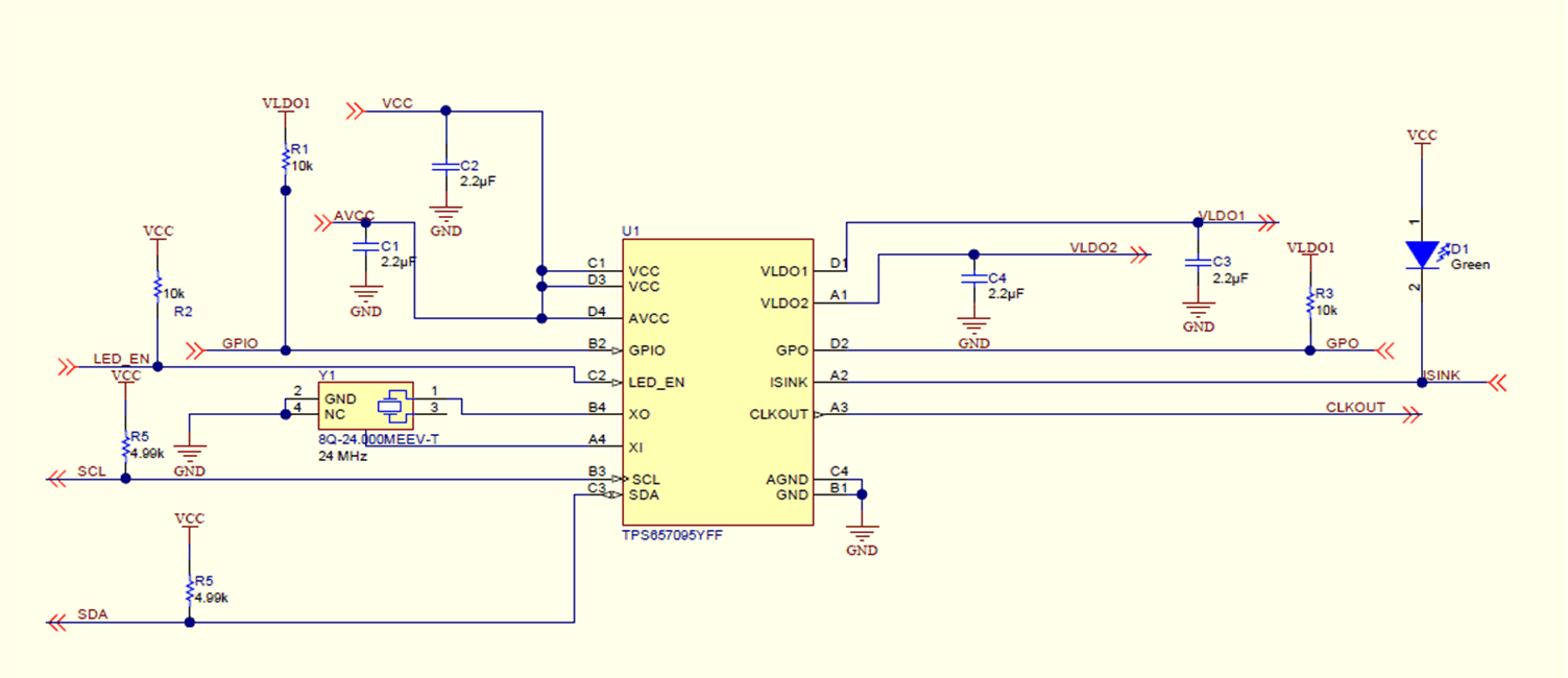 Figure 30. Application Schematic
8.2.1 Design Requirements
Table 18. Design Parameters
| DESIGN PARAMETER | VALUE |
|---|---|
| Typical Input Voltage | 5V |
| LDO1 Output Voltage | 1.8V (off by default) |
| LDO2 Output Voltage | 1.2V (off by default) |
8.2.2 Detailed Design Procedure
8.2.2.1 Output Capacitor Selection
The control loop of the LDOs is internally compensated such that they operate with small ceramic output capacitors of 2.2µF.
8.2.2.2 Input Capacitor Selection
A low ESR input capacitor is required for best input voltage filtering and minimizing the interference with other circuits. The LDOs need a ceramic input capacitor with a minimum capacitance of 1.0µF. The input capacitor can be increased without any limit for better input voltage filtering.
Table 19. Tested Capacitors
| TYPE | VALUE | VOLTAGE RATING | SIZE | SUPPLIER | MATERIAL |
|---|---|---|---|---|---|
| GRM155R60J225ME15D | 2.2 µF | 6.3 V | 0402 | Murata | Ceramic X5R |
| GRM185R60J225 | 2.2 µF | 6.3 V | 0603 | Murata | Ceramic X5R |
| GRM185R60J105K | 1 µF | 6.3 V | 0603 | Murata | Ceramic X5R |
8.2.3 Application Curves
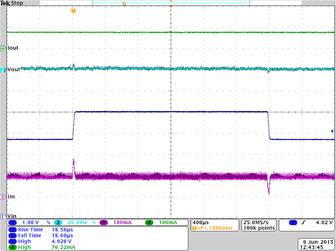
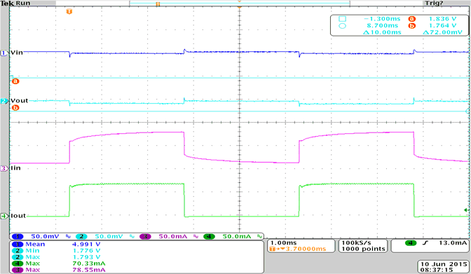
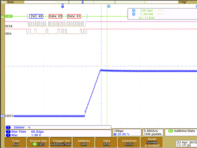
The graphs below were taken using the TPS657095EVM with the passive components as listed below:
- CIN(VCC) = GRM185R60J105K (1 µF / 6.3V)
- COUT(LDO1) = COUT(LDO2) = GRM185R60J225 (2.2 µF / 6.3 V)
- VCC = 5 V unless otherwise noted
Table 20. Table of Graphs
| DESCRIPTION | FIGURE | |
|---|---|---|
| Line Transient Response LDO1 | VCC = 3.6V to 5V to 3.6V; IOUT = 75mA; VOUT = 1.8V | Figure 31 |
| Line Transient Response LDO2 | VCC = 3.6V to 5V to 3.6V; IOUT = 75mA; VOUT = 2.8V | Figure 32 |
| Load Transient Response LDO1 | VCC = 5V; IOUT = 7.5mA to 68mA to 7.5mA; VOUT = 1.8V |
Figure 33 |
| Load Transient Response LDO2 | VCC = 5V; IOUT = 7.5mA to 68mA to 7.5mA; VOUT = 2.8V | Figure 34 |
| LDO1 and LDO2 Start-up Timing | VCC = 5V; IOUT = 0mA | Figure 35 |
| LDO1 and LDO2 Start-up Timing | VCC = 5V; IOUT = 75mA | Figure 36 |
| Duty Cycle on CLKout vs Programmed Frequency | VCC = 5V; f(crystal) = 24MHz; VLDO1 = 1.8V | Figure 37 |
| Period Jitter on CLKout vs Temperature and Output Frequency | VCC = 5V; f(crystal) = 24MHz; VLDO1 = 1.8V | Figure 38 |
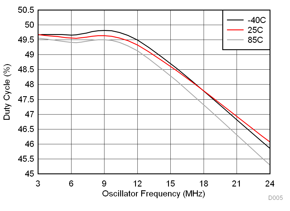
| VCC = 5 V, VLDO1 = 1.8 V, fCrystal = 24 MHz |


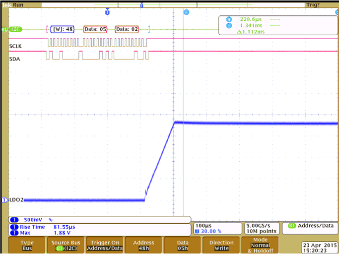
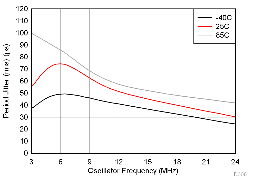
| VCC = 5 V |