SLVS979C October 2009 – May 2018 TPS65720 , TPS65721
PRODUCTION DATA.
- 1 Features
- 2 Applications
- 3 Description
- 4 Revision History
- 5 Device Options
- 6 Pin Configuration and Functions
- 7 Specifications
-
8 Detailed Description
- 8.1 Overview
- 8.2 Functional Block Diagrams
- 8.3
Feature Description
- 8.3.1 Battery Charger and Power Path
- 8.3.2 Power-Path Management
- 8.3.3 Battery Charging
- 8.3.4 Thermal Regulation and Thermal Shutdown
- 8.3.5 Battery Pack Temperature Monitoring
- 8.3.6 DCDC1 Converter
- 8.3.7 Power Save Mode
- 8.3.8 Short-Circuit Protection
- 8.3.9 Thermal Shutdown
- 8.3.10 LDO1
- 8.4 Device Functional Modes
- 8.5 Programming
- 8.6
Register Maps
- 8.6.1 CHGSTATUS Register Address: 01h (read only)
- 8.6.2 CHGCONFIG0 Register Address: 02h (read/write)
- 8.6.3 CHGCONFIG1 Register Address: 03h (read/write)
- 8.6.4 CHGCONFIG2 Register Address: 04h (read/write)
- 8.6.5 CHGCONFIG3 Register Address: 05h (read/write)
- 8.6.6 CHGSTATE Register Address: 06h (read only)
- 8.6.7 DEFDCDC1 Register Address: 07h (read/write)
- 8.6.8 LDO_CTRL Register Address: 08h (read/write)
- 8.6.9 CONTROL0 Register Address: 09h (read/write)
- 8.6.10 CONTROL1 Register Address: 0Ah (read/write)
- 8.6.11 GPIO_SSC Register Address: 0Bh (read/write)
- 8.6.12 GPIODIR Register Address: 0Ch (read/write)
- 8.6.13 IRMASK0 Register Address: 0Dh (read/write)
- 8.6.14 IRMASK1 Register Address: 0Eh (read/write)
- 8.6.15 IRMASK2 Register Address: 0Fh (read/write)
- 8.6.16 IR0 Register Address: 10h (read only)
- 8.6.17 IR1 Register Address: 11h (read)
- 8.6.18 IR2 Register Address: 12h (read)
- 9 Application and Implementation
- 10Power Supply Recommendations
- 11Layout
- 12Device and Documentation Support
- 13Mechanical, Packaging, and Orderable Information
Package Options
Mechanical Data (Package|Pins)
- YFF|25
Thermal pad, mechanical data (Package|Pins)
Orderable Information
8.3.3 Battery Charging
When <CH_EN> = 1, battery charging begins. First, the device checks for a short circuit on the BAT pin by sourcing IBAT(SC) to the battery and monitoring the voltage. When the BAT voltage exceeds VBAT(SC), the battery charging continues. The battery is charged in three phases: conditioning pre-charge, constant-current fast charge (current regulation) and a constant-voltage tapering (voltage regulation). In all charge phases, an internal control loop monitors the IC junction temperature and reduces the charge current if an internal temperature threshold is exceeded.
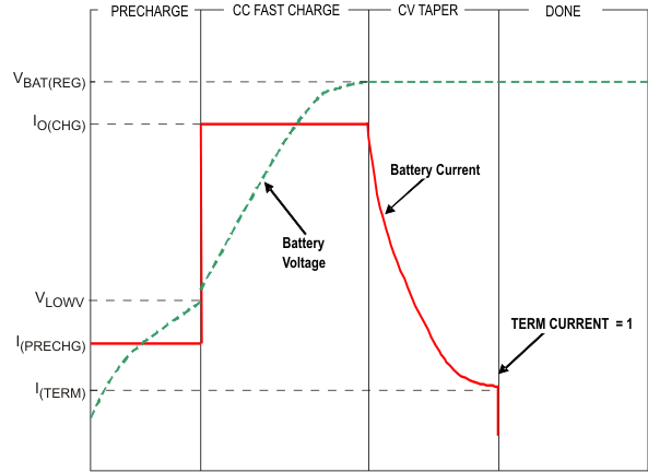
Figure 11 shows what happens in each of the three phases:
 Figure 11. Battery Charge
In the pre-charge phase, the battery is charged with the pre-charge current (IPRECHG). Once the battery voltage crosses the VLOWV threshold, the battery is charged with the fast-charge current (ICHG). As the battery voltage reaches VBAT(REG), the battery is held at a constant voltage of VBAT(REG) and the charge current tapers off as the battery approaches full charge. Note that termination detection is disabled whenever the charge rate is reduced from the set point because of the actions of the thermal loop, the DPM loop, or the VIN(LOW) loop. The value of the fast-charge current is set by the resistor connected from the ISET pin to GND, and is given by Equation 1:
The charge current limit is adjustable up to 300 mA. The valid resistor range is 1500 Ω to 11.25 kΩ. Note that if ICHG is programmed as greater than the input current limit, the battery does not charge at the rate of ICHG, but at the slower rate of IACmax (minus the load current on the OUT pin, if any). In this case, the charger timers are proportionately slowed down.