SWCS048G March 2010 – September 2014 TPS65921
PRODUCTION DATA.
- 1Device Overview
- 2Revision History
- 3Terminal Configuration and Functions
-
4Specifications
- 4.1 Absolute Maximum Ratings
- 4.2 Handling Ratings
- 4.3 Recommended Operating Conditions
- 4.4 Thermal Resistance Characteristics for ZQZ Package
- 4.5 Crystal Oscillator
- 4.6 Clock Slicer
- 4.7 32KCLKOUT Output Clock
- 4.8 HFCLKOUT Output Clock
- 4.9 VDD1 DC-DC Converter
- 4.10 VDD2 DC-DC Converter
- 4.11 VIO DC-DC Converter
- 4.12 VMMC1 Low Dropout Regulator
- 4.13 VDAC Low Dropout Regulator
- 4.14 VAUX2 Low Dropout Regulator
- 4.15 VPLL1 Low Dropout Regulator
- 4.16 Internal LDOs
- 4.17 Voltage References
- 4.18 Battery Threshold Levels
- 4.19 Power Consumption
- 4.20 USB Charge Pump
- 4.21 Hot-Die Detection and Thermal Shutdown
- 4.22 USB
- 4.23 MADC
- 4.24 TPS65921 Interface Target Frequencies
- 4.25 JTAG Interfaces
- 5Detailed Description
- 6Device and Documentation Support
- 7Mechanical Packaging and Orderable Information
Package Options
Mechanical Data (Package|Pins)
Thermal pad, mechanical data (Package|Pins)
Orderable Information
3 Terminal Configuration and Functions
shows the ball locations for the 120-ball plastic ball grid array (PBGA) package and is used in conjunction with ball description to locate signal names and ball grid numbers.
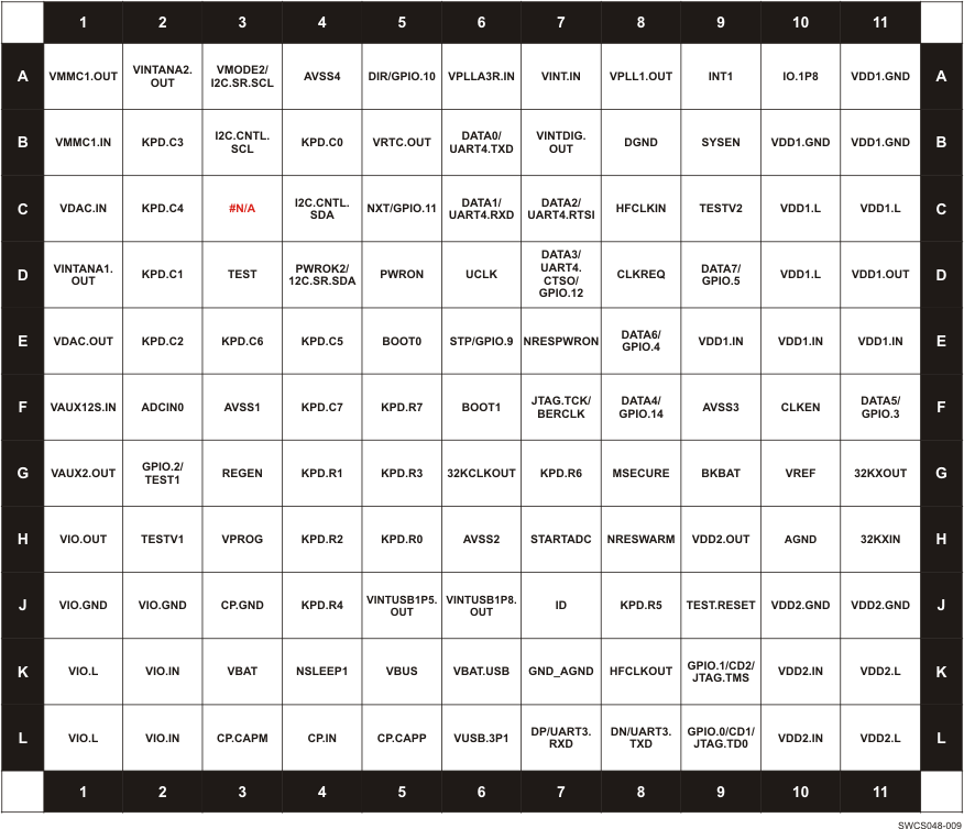 Figure 3-1 Ball Placement (Top View)
3.1 Signal Descriptions
Table 3-1 Signal Descriptions
| NAME | BALL | SUPPLIES | TYPE | I/O | DESCRIPTION | PU/PD |
|---|---|---|---|---|---|---|
| ADCIN0 | F2 | Analog | I/O | General-purpose ADC input | NO | |
| STARTADC | H7 | VDDIO/DGND | Digital | I | ADC conversion request/JTAG test data input | NO |
| I2C.CNTL.SDA | C4 | VDDIO/DGND | Digital | I/O | I2C bidirectional data signal | External PU |
| I2C.CNTL.SCL | B3 | VDDIO/DGND | Digital | I/O | I2C bidirectional clock signal | External PU |
| I2C.SR.SDA | D4 | VDDIO/DGND | Digital | I/O | HS I2C bidirectional data signal | External PU |
| I2C.SR.SCL | A3 | VDDIO/DGND | Digital | I/O | HS I2C bidirectional Clock signal | External PU |
| PWRON | D5 | VBAT/GND | Digital | I | Input detects a control command to start or stop the system. | External PU |
| REGEN | G3 | Digital | O | Enable signal for external LDO | PU | |
| MSECURE | G8 | VDDIO/DGND | Digital | I | Security and digital rights management | NO |
| BOOT0 | E5 | VBAT/GND | Digital | I | Power-up sequence selection | Programmable PD (default active) |
| BOOT1 | F6 | VBAT/GND | Digital | I | Power-up sequence selection | Programmable PD (default active) |
| NRESPWRON | E7 | VDDIO/DGND | Digital | O | Output control the NRESPWRON of the application processor | NO |
| NRESWARM | H8 | VDDIO/DGND | Digital | I | Warm reset signal | PU |
| NSLEEP1 | K4 | VDDIO/DGND | Digital | I | ACTIVE-SLEEP state transition control signal | NO |
| INT1 | A9 | VDDIO/DGND | Digital | O | Output line interrupt | NO |
| SYSEN | B9 | VDDIO/DGND | Digital | O | System enable output | NO |
| CLKEN | F10 | VDDIO/DGND | Digital | O | Clock Enable | NO |
| 32KCLKOUT | G6 | VDDIO/DGND | Digital | O | 32-kHz clock output | PD disabled in ACTIVE state |
| 32KXOUT | G11 | VRTC/REFGND | Analog | I | 32-kHz crystal oscillator | NO |
| 32KXIN | H11 | VRTC/REFGND | Analog | I | 32-kHz crystal oscillator | NO |
| HFCLKIN | C8 | VDDIO/DGND | Analog | I | Sine wave or square wave input | NO |
| HFCLKOUT | K8 | VDDIO/DGND | Digital | O | 50% duty cycle square wave output | NO |
| VREF | G10 | VREF/REFGND | Analog | O | Bandgap voltage | NO |
| GND_AGND | K7 | AGND | Analog | I/O | Substrate ground | NO |
| AGND | H10 | REFGND | Analog | I/O | Reference ground | NO |
| DGND | B8 | DGND | Power | I/O | Digital ground | NO |
| IO.1P8 | A10 | Power | I | Supply for I/O buffers (VDDIO) | NO | |
| BKBAT | G9 | VBACKUP/AGND | Power | I | Not used. Must be grounded | NO |
| VDD1.IN | E9, E10, E11 | Power | I | VDD1 DC-DC input | NO | |
| VDD1.GND | A11, B10, B11 | Power | I/O | VDD1 DC-DC power ground | NO | |
| VDD1.L | C10, C11, D10 | Power | O | VDD1 DC-DC switched output | NO | |
| VDD1.OUT | D11 | Analog | I | VDD1 feedback voltage | PD | |
| VDD2.IN | K10, L10 | Power | I | VDD2 DC-DC input | NO | |
| VDD2.GND | J10, J11 | Power | I/O | VDD2 DC-DC power ground | NO | |
| VDD2.L | K11, L11 | Power | O | VDD2 DC-DC switched output | NO | |
| VDD2.OUT | H9 | Analog | I | VDD2 feedback voltage | PD | |
| VIO.IN | K2, L2 | Power | I | VIO DC-DC input | NO | |
| VIO.GND | J1, J2 | Power | I/O | VIO DC-DC power ground | NO | |
| VIO.L | K1, L1 | Power | O | VIO DC-DC switched output | NO | |
| VIO.OUT | H1 | Analog | I | VIO feedback voltage | PD | |
| VAUX12S.IN | F1 | Power | I | VAUX2 LDO input | NO | |
| VAUX2.OUT | G1 | Power | O | VAUX2 regulator output | PD | |
| VPLLA3R.IN | A6 | Power | I | VPLL1/VRTC LDO input | NO | |
| VPLL1.OUT | A8 | Power | O | VPLL1 LDO regulator output | PD | |
| VRTC.OUT | B5 | Power | O | VRTC internal LDO regulator output (internal use only) | PD | |
| VINT.IN | A7 | Power | I | VINTDIG LDO input | NO | |
| VINTANA1.OUT | D1 | Power | O | VINTANA1 internal LDO regulator output (internal use only) | PD | |
| VINTANA2.OUT | A2 | Power | O | VINTANA2 internal LDO regulator output (internal use only) | PD | |
| VDAC.IN | C1 | Power | I | VDAC/VINTANA1/VINTAN2 LDO input | NO | |
| VDAC.OUT | E1 | Power | O | VDAC LDO regulator output | PD | |
| VINTDIG.OUT | B7 | Power | O | VINTDIG internal LDO regulator output (internal use only) | PD | |
| VMMC1.OUT | A1 | Power | O | VMMC1 LDO regulator output | PD | |
| VBAT.USB | K6 | Power | I | VINTUSBiP5,VINTUSB1P8,VUSB.3P1 input regulator | NO | |
| VUSB.3P1 | L6 | Power | O | VUSB.3P1 LDO regulator output | PD | |
| VINTUSB1P8.OUT | J6 | Power | O | VUSB1P8 LDO regulator output (internal use only) | PD | |
| VINTUSB1P5.OUT | J5 | Power | O | VUSB1P5 LDO regulator output (internal use only) | PD | |
| TESTV1 | H2 | Analog | IO | Analog test pin 1 | NO | |
| TESTV2 | C9 | Analog | IO | Analog test pin 2 | NO | |
| TEST | D3 | VDDIO/DGND | Digital | IO | Selection between JTAG mode and application mode | PD |
| AVSS1 | F3 | AGND | Power | I/O | Analog ground | NO |
| AVSS2 | H6 | AGND | Power | I/O | Analog ground | NO |
| AVSS3 | F9 | AGND | Power | I/O | Analog ground | NO |
| AVSS4 | A4 | AGND | Power | I/O | Analog ground | NO |
| VBUS | K5 | Power | VBUS power rail | NO | ||
| DP/UART3.RXD | L7 | Analog | I/O | USB differential data line | NO | |
| DN/UART3.TXD | L8 | Analog | I/O | USB differential data line | NO | |
| ID | J7 | VDDIO/DGND | Digital | I/O | USB ID | NO |
| UCLK | D6 | VDDIO/DGND | Digital | I/O | HS USB Clock | NO |
| STP/GPIO.9 | E6 | VDDIO/DGND | Digital | I/O | HS USB Stop | NO |
| DIR/GPIO.10 | A5 | VDDIO/DGND | Digital | I/O | HS USB Direction | NO |
| NXT/GPIO.11 | C5 | VDDIO/DGND | Digital | I/O | HS USB Next | NO |
| DATA0/UART4.TXD | B6 | VDDIO/DGND | Digital | I/O | HS USB Data0 | NO |
| DATA1/UART4.RXD | C6 | VDDIO/DGND | Digital | I/O | HS USB Data1 | NO |
| DATA2/UART4.RTSI | C7 | VDDIO/DGND | Digital | I/O | HS USB Data2 | NO |
| DATA3/UART4.CTSO/GPIO.12 | D7 | VDDIO/DGND | Digital | I/O | HS USB Data3 | NO |
| DATA4/GPIO.14 | F8 | VDDIO/DGND | Digital | I/O | HS USB Data4 | NO |
| DATA5/GPIO.3 | F11 | VDDIO/DGND | Digital | I/O | HS USB Data5 | NO |
| DATA6/GPIO.4 | E8 | VDDIO/DGND | Digital | I/O | HS USB Data6 | NO |
| DATA7/GPIO.5 | D9 | VDDIO/DGND | Digital | I/O | HS USB Data7 | NO |
| CP.IN | L4 | Power | I/O | Charge pump input voltage | NO | |
| CP.GND | J3 | Power Gnd | I/O | Charge pump ground | NO | |
| CP.CAPP | L5 | Analog | I/O | Charge pump flying capacitor P | NO | |
| CP.CAPM | L3 | Analog | I/O | Charge pump flying capacitor M | NO | |
| KPD.C0 | B4 | VDDIO/DGND | Open Drain | O | Keypad column 0 | PU |
| KPD.C1 | D2 | VDDIO/DGND | Open Drain | O | Keypad column 1 | PU |
| KPD.C2 | E2 | VDDIO/DGND | Open Drain | O | Keypad column 2 | PU |
| KPD.C3 | B2 | VDDIO/DGND | Open Drain | O | Keypad column 3 | PU |
| KPD.C4 | C2 | VDDIO/DGND | Open Drain | O | Keypad column 4 | PU |
| KPD.C5 | E4 | VDDIO/DGND | Open Drain | O | Keypad column 5 | PU |
| KPD.C6 | E3 | VDDIO/DGND | Open Drain | O | Keypad column 6 | PU |
| KPD.C7 | F4 | VDDIO/DGND | Open Drain | O | Keypad column 7 | PU |
| KPD.R0 | H5 | VDDIO/DGND | Digital | I | Keypad row 0 | PU |
| KPD.R1 | G4 | VDDIO/DGND | Digital | I | Keypad row 1 | PU |
| KPD.R2 | H4 | VDDIO/DGND | Digital | I | Keypad row 2 | PU |
| KPD.R3 | G5 | VDDIO/DGND | Digital | I | Keypad row 3 | PU |
| KPD.R4 | J4 | VDDIO/DGND | Digital | I | Keypad row 4 | PU |
| KPD.R5 | J8 | VDDIO/DGND | Digital | I | Keypad row 5 | PU |
| KPD.R6 | G7 | VDDIO/DGND | Digital | I | Keypad row 6 | PU |
| KPD.R7 | F5 | VDDIO/DGND | Digital | I | Keypad row 7 | PU |
| VBAT | K3 | Power | I/O | Battery input voltage (Sense) | NO | |
| CLKREQ | D8 | VDDIO/DGND | Digital | I | Clock request line | PD |
| TEST.RESET | J9 | VBAT/GND | Digital | I | Reset the device (except the state-machine) | PD |
| VPROG | H3 | Analog | I | Reserved. Must be grounded. | NO | |
| JTAG/TCK/BERCLK | F7 | VDDIO/DGND | Digital | I | JTAG clock input | NO |
| GPIO.0/CD1/JTAG.TDO | L9 | VDDIO/DGND | Digital | I/O | JTAG test output or GPIO0/card detection 1 | PD |
| GPIO.1/CD2/JTAG.TMS | K9 | VDDIO/DGND | Digital | I/O | JTAG test mode state or GPIO1/card detection 2 | PD |
| GPIO.2/TEST1 | G2 | VDDIO/DGND | Digital | I | GPIO/Digital test pin | Programmable PD |
| VMMC1.IN | B1 | Power | I | VMMC1 input LDO | NO | |
| N/A | C3 | N/A | N/A | N/A | N/A | N/A |