SWCS037I May 2008 – January 2015 TPS65920 , TPS65930
PRODUCTION DATA.
- 1Device Overview
- 2Revision History
- 3Terminal Configuration and Functions
- 4Specifications
-
5Detailed Description
- 5.1
Power Module
- 5.1.1 Power Providers
- 5.1.2 Power References
- 5.1.3 Power Control
- 5.1.4 Power Consumption
- 5.1.5 Power Management
- 5.2 Real-Time Clock and Embedded Power Controller
- 5.3 USB Transceiver
- 5.4 MADC
- 5.5 LED Drivers
- 5.6 Keyboard
- 5.7 Clock Specifications
- 5.8 Debouncing Time
- 5.9 External Components
- 5.1
Power Module
-
6Audio/Voice Module (TPS65930 Device Only)
- 6.1 Audio/Voice Downlink (RX) Module
- 6.2 Audio Uplink (TX) Module
- 7Device and Documentation Support
- 8Mechanical, Packaging, and Orderable Information
Package Options
Mechanical Data (Package|Pins)
- ZCH|139
Thermal pad, mechanical data (Package|Pins)
Orderable Information
6 Audio/Voice Module (TPS65930 Device Only)
NOTE
This section applies only to the TPS65930 device.
Figure 6-1 is the audio/voice module block diagram.
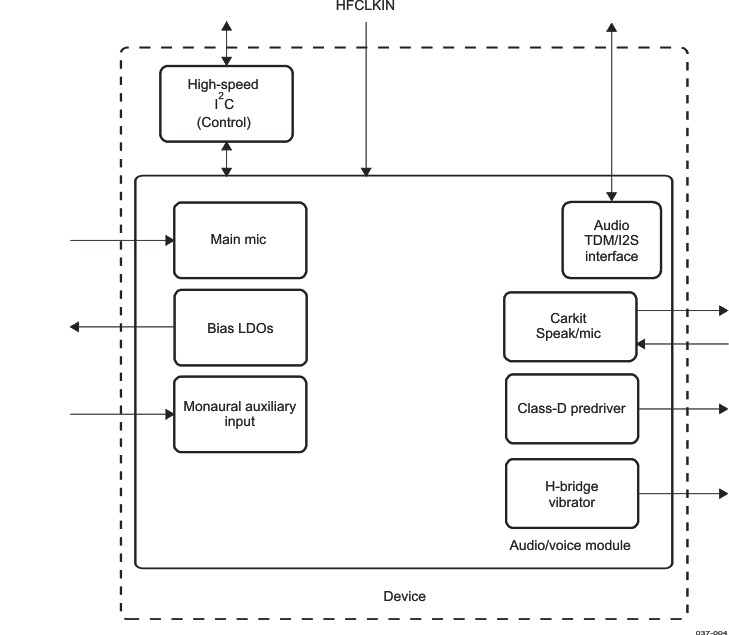 Figure 6-1 Audio/Voice Module Block Diagram
6.1 Audio/Voice Downlink (RX) Module
The audio/voice module includes the following output stages:
- Predriver output signals for external class-D amplifiers (single-ended)
- Vibrator H-bridge
6.1.1 Predriver for External Class-D Amplifier
The external class-D amplifiers provide a stereo signal on terminals PreD.LEFT and PreD.RIGHT to drive the external class-D amplifier. These terminals are available if a stereo, single-ended, ac-coupled headset is used.
6.1.1.1 Predriver Output Characteristics
Table 6-1 lists the predriver output characteristics.
Table 6-1 Predriver Output Characteristics
| PARAMETER | TEST CONDITIONS | MIN | TYP | MAX | UNIT |
|---|---|---|---|---|---|
| Load impedance | 10 | kΩ | |||
| 50 | pF | ||||
| Gain range (2) | Audio path | –92 | 30 | dB | |
| Voice path | –66 | 30 | |||
| Absolute gain error | –1 | 1 | dB | ||
| Peak-to-peak output voltage (0 dBFs) | Default gain (1) | 1.5 | VPP | ||
| Total harmonic distortion | At 0 dBFs | –80 | –75 | dB | |
| Default gain (1) | At –6 dBFs | –74 | –69 | ||
| Load > 10 kΩ // 50 pF | At –20 dBFs | –70 | –65 | ||
| At –60 dBFs | –30 | –25 | |||
| Idle channel noise (20 Hz to 20 kHz, A-weighted) | Default gain (1)
Load = 10 Ω |
–90 | –85 | dB | |
| SNR (A-weighted over 20-kHz bandwidth) | At 0 dBFs | 83 | 88 | dB | |
| Default gain(1) | At –60 dBFs | 30 | |||
| Output PSRR (for all gains) | 20 Hz to 4 kHz | 90 | dB | ||
| 20 Hz to 20 kHz | 70 |
Voice digital filter = –3 to 12 dB (1-dB steps)
ARXPGA (volume control) = –24 to 12 dB (2-dB steps)
Output driver = –6 dB, 0 dB, 6 dB
6.1.1.2 External Components and Application Schematics
Figure 6-2 is a simplified schematic for the external class-D predriver.
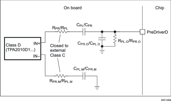
NOTE
For other component values, see Table 5-48.
6.1.2 Vibrator H-Bridge
A digital signal from the pulse width modulated generator is fed to the vibrator H-bridge driver. The vibrator H-bridge is a differential driver that drives vibrator motors. The differential output allows dual rotation directions.
6.1.2.1 Vibrator H-Bridge Output Characteristics
Table 6-2 lists the vibrator H-bridge output characteristics.
Table 6-2 Vibrator H-Bridge Output Characteristics
| PARAMETER | Test Conditions | MIN | TYP | MAX | UNIT |
|---|---|---|---|---|---|
| VBAT voltage | 2.8 | 3.6 | 4.8 | V | |
| Differential output swing (16-Ω load) | VBAT = 2.8 V | 3.6 | VPP | ||
| VBAT = 3.5 V | 4.3 | ||||
| Output resistance (summed for both sides) | 8 | Ω | |||
| Load capacitance | 100 | pF | |||
| Load resistance | 8 | 16 | 60 | Ω | |
| Load inductance | 30 | 300 | μH | ||
| Total harmonic distortion | 10% | ||||
| Operating frequency | 20 | 10k | Hz |
6.1.2.2 External Components and Application Schematics
Figure 6-3 is a simplified vibrator H-bridge schematic.
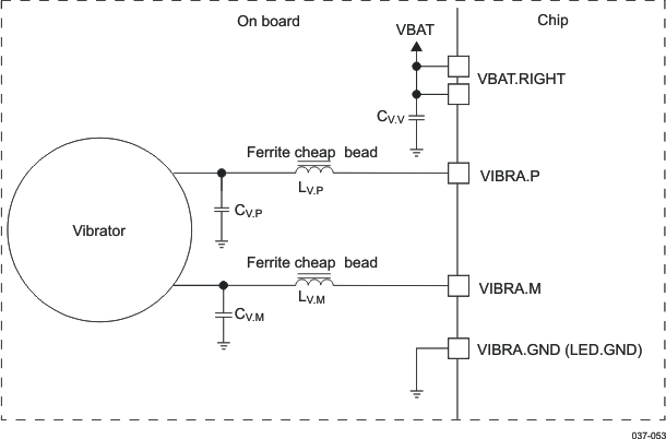 Figure 6-3 Vibrator H-Bridge
NOTE
For other component values, see Table 5-48.
Example of ferrite: BLM 18BD221SN1.
6.1.3 Carkit Output
The USB-CEA carkit uses the DP/DM pad to output audio signals (see the CEA-936–Mini-USB Analog Carkit specification).
Figure 6-4 shows the carkit output downlink full path characteristics for audio and USB.
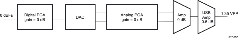 Figure 6-4 Carkit Output Downlink Path Characteristics
Table 6-3 lists the USB-CEA carkit audio downlink electrical characteristics.
Table 6-3 USB-CEA Carkit Audio Downlink Electrical Characteristics
| PARAMETER | CONDITIONS | MIN | TYP | MAX | UNIT |
|---|---|---|---|---|---|
| Output load | USB-CEA (DP/DM) | 20 | kΩ | ||
| Gain range(2) | Audio path | –92 | 30 | dB | |
| Voice path | –66 | 30 | |||
| Absolute gain error | At 1 kHz | –1 | 1 | dB | |
| Peak-to-peak differential output voltage (0 dBFs) | Gain = 0 dB | 1.5 | VPP | ||
| Total harmonic distortion | At 0 dBFs | –80 | –75 | dB | |
| At –6 dBFs | –74 | –69 | |||
| At –20 dBFs | –70 | –65 | |||
| At –60 dBFs | –30 | –25 | |||
| THD+N (20 Hz to 20 kHz, A-weighted) | At 0 dBFs | 60 | dB | ||
| Idle channel noise (20 Hz to 20 kHz, A-weighted) | Default gain(1) | –90 | –85 | dB | |
| Output PSRR | 20 Hz to 20 kHz | 60 | dB | ||
| Supply voltage (Vintana1) | 1.5 | V | |||
| Common mode output voltage for USB-CEA | 1.3 | 1.35 | 1.4 | V | |
| Isolation between D+/D– during audio mode (20 Hz to 20 kHz) | 60 | dB | |||
| Crosstalk between right and left channels | USB-CEA stereo | –90 | dB | ||
| Crosstalk RX/Tx (1 VPP output) | USB-CEA mono/stereo | –60 | dB | ||
| Signal noise ratio (20 Hz to 20 kHz, A-weighted) | At 0 dBFs | 60 | dB | ||
| Phone speaker amplifier output impedance at 1 kHz | USB-CEA (DP/DM) | 200 | Ω |
Voice digital filter = –36 to 12 dB (1-dB steps)
ARXPGA (volume control) = –24 to 12 dB (2-dB steps)
Output driver (USB-CEA) = –1 dB
6.1.4 Digital Audio Filter Module
Figure 6-5 shows the digital audio filter downlink full path characteristics for the audio interface.
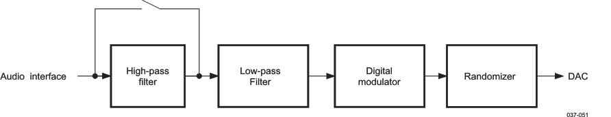 Figure 6-5 Digital Audio Filter Downlink Path Characteristics
The HPF can be bypassed. It is controlled by the MISC_SET_2 ARX_HPF_BYP bit set to address 0x49.
Table 6-4 lists the audio filter frequency responses relative to reference gain at 1 kHz.
Table 6-4 Digital Audio Filter RX Electrical Characteristics
| PARAMETER | CONDITIONS | MIN | TYP | MAX | UNIT |
|---|---|---|---|---|---|
| Passband | 0.42 | FS | |||
| Passband ripple | 0 to 0.42FS(1) | –0.25 | 0.1 | 0.25 | dB |
| Stopband | 0.6 | FS | |||
| Stopband attenuation | F = 0.6FS(1) to 0.8FS(1) | 60 | 75 | dB | |
| Group delay | 15.8/FS(1) | μs | |||
| Linear phase | –1.4 | 1.4 | ° |
6.1.5 Boost Stage
The boost effect adds emphasis to low frequencies. It compensates for a HPF created by the capacitor resistor (CR) filter of the headset (in ac-coupling configuration).
There are four modes. Three effects are available, with slightly different frequency responses, and the fourth setting disables the boost effect:
- Boost effect 1
- Boost effect 2
- Boost effect 3
- Flat equalization: The boost effect is in bypass mode.
NOTE
Boost effect modes are defined in Table 6-5.
Table 6-5 and Table 6-6 include the typical values according to the frequency response versus input frequency and FS frequency.
Table 6-5 Boost Electrical Characteristics Versus FS Frequency (FS ≤ 22.05 kHz)
| FREQUENCY (Hz) |
FS = 8 kHz | FS = 11.025 kHz | FS = 12 kHz | FS = 16 kHz | FS = 22.05 kHz | UNIT | ||||||||||
|---|---|---|---|---|---|---|---|---|---|---|---|---|---|---|---|---|
| 1 | 2 | 3 | 1 | 2 | 3 | 1 | 2 | 3 | 1 | 2 | 3 | 1 | 2 | 3 | ||
| 10 | 4.51 | 5.13 | 5.62 | 5.10 | 5.51 | 5.80 | 5.22 | 5.58 | 5.83 | 5.54 | 5.77 | 5.92 | 5.76 | 5.89 | 5.97 | dB |
| 12 | 4.08 | 4.83 | 5.46 | 4.80 | 5.32 | 5.71 | 4.95 | 5.41 | 5.76 | 5.36 | 5.66 | 5.87 | 5.65 | 5.83 | 5.94 | |
| 15.2 | 3.43 | 4.32 | 5.18 | 4.28 | 4.97 | 5.54 | 4.47 | 5.11 | 5.61 | 5.03 | 5.47 | 5.79 | 5.45 | 5.71 | 5.90 | |
| 18.2 | 2.91 | 3.86 | 4.89 | 3.82 | 4.63 | 5.36 | 4.04 | 4.80 | 5.45 | 4.71 | 5.26 | 5.69 | 5.24 | 5.59 | 5.84 | |
| 20.5 | 2.56 | 3.53 | 4.65 | 3.49 | 4.37 | 5.21 | 3.72 | 4.56 | 5.32 | 4.45 | 5.09 | 5.60 | 5.06 | 5.49 | 5.79 | |
| 29.4 | 1.62 | 2.49 | 3.78 | 2.45 | 3.42 | 4.57 | 2.68 | 3.74 | 4.73 | 3.51 | 4.39 | 5.24 | 4.35 | 5.02 | 5.59 | |
| 39.7 | 1.05 | 1.71 | 2.93 | 1.67 | 2.55 | 3.84 | 1.88 | 2.80 | 4.06 | 2.66 | 3.63 | 4.72 | 3.67 | 4.45 | 5.27 | |
| 50.4 | 0.71 | 1.20 | 2.26 | 1.17 | 1.91 | 3.17 | 1.33 | 2.13 | 3.41 | 2.01 | 2.95 | 4.19 | 2.89 | 3.85 | 4.88 | |
| 60.3 | 0.51 | 0.92 | 1.79 | 0.89 | 1.49 | 2.65 | 1.00 | 1.68 | 2.89 | 1.57 | 2.43 | 3.72 | 2.39 | 3.35 | 4.52 | |
| 76.7 | 0.32 | 0.61 | 1.26 | 0.59 | 1.05 | 1.99 | 0.69 | 1.18 | 2.22 | 1.11 | 1.79 | 3.04 | 1.76 | 2.66 | 3.94 | |
| 97.5 | 0.20 | 0.39 | 0.87 | 0.38 | 0.70 | 1.43 | 0.44 | 0.79 | 1.62 | 0.75 | 1.27 | 2.36 | 1.24 | 2.00 | 3.28 | |
| 131.5 | 0.12 | 0.21 | 0.50 | 0.20 | 0.39 | 0.88 | 0.25 | 0.47 | 1.02 | 0.42 | 0.78 | 1.59 | 0.75 | 1.30 | 2.41 | |
| 157 | 0.08 | 0.15 | 0.36 | 0.15 | 0.28 | 0.65 | 0.17 | 0.33 | 0.75 | 0.31 | 0.57 | 1.22 | 0.55 | 0.99 | 1.93 | |
| 200 | 0.05 | 0.09 | 0.22 | 0.09 | 0.17 | 0.41 | 0.11 | 0.21 | 0.49 | 0.19 | 0.37 | 0.82 | 0.36 | 0.66 | 1.38 | |
| 240 | 0.03 | 0.06 | 0.15 | 0.06 | 0.12 | 0.29 | 0.07 | 0.14 | 0.35 | 0.14 | 0.26 | 0.60 | 0.25 | 0.48 | 1.04 | |
| 304 | 0.02 | 0.04 | 0.09 | 0.04 | 0.07 | 0.18 | 0.04 | 0.09 | 0.22 | 0.08 | 0.16 | 0.38 | 0.16 | 0.30 | 0.70 | |
| 463 | 0.00 | 0.01 | 0.03 | 0.01 | 0.03 | 0.07 | 0.02 | 0.04 | 0.09 | 0.03 | 0.07 | 0.17 | 0.07 | 0.13 | 0.32 | |
| 704 | 0.00 | 0.00 | 0.01 | 0.00 | 0.01 | 0.03 | 0.01 | 0.01 | 0.03 | 0.01 | 0.03 | 0.07 | 0.03 | 0.06 | 0.14 | |
| 1008 | 0.00 | 0.00 | 0.00 | 0.00 | 0.00 | 0.01 | 0.00 | 0.00 | 0.01 | 0.00 | 0.01 | 0.03 | 0.01 | 0.02 | 0.06 | |
| 1444 | 0.00 | 0.00 | 0.00 | 0.00 | 0.00 | 0.00 | 0.00 | 0.00 | 0.00 | 0.00 | 0.00 | 0.00 | 0.00 | 0.01 | 0.02 | |
| 2070 | 0.00 | 0.00 | 0.00 | 0.00 | 0.00 | 0.00 | 0.00 | 0.00 | 0.00 | 0.00 | 0.00 | 0.00 | 0.00 | 0.00 | 0.01 | |
| 3770 | 0.00 | 0.00 | 0.00 | 0.00 | 0.00 | 0.00 | 0.00 | 0.00 | 0.00 | 0.00 | 0.00 | 0.00 | 0.00 | 0.00 | 0.00 | |
Table 6-6 Boost Electrical Characteristics Versus FS Frequency (FS ≥ 24 kHz)
| FREQUENCY (Hz) |
FS = 24 kHz | FS = 32 kHz | FS = 44.1 kHz | FS = 48 kHz | FS = 96 kHz | UNIT | ||||||||||
|---|---|---|---|---|---|---|---|---|---|---|---|---|---|---|---|---|
| 1 | 2 | 3 | 1 | 2 | 3 | 1 | 2 | 3 | 1 | 2 | 3 | 1 | 2 | 3 | ||
| 10 | 5.79 | 5.90 | 5.97 | 5.89 | 5.89 | 5.99 | 5.95 | 5.98 | 6.04 | 5.96 | 5.99 | 6.01 | 5.71 | 5.83 | 5.90 | dB |
| 12 | 5.70 | 5.85 | 5.95 | 5.84 | 5.84 | 5.98 | 5.92 | 5.97 | 6.03 | 5.94 | 5.98 | 6.00 | 5.54 | 5.68 | 5.81 | |
| 15.2 | 5.53 | 5.76 | 5.91 | 5.73 | 5.73 | 5.96 | 5.87 | 5.94 | 6.02 | 5.89 | 5.95 | 5.99 | 5.40 | 5.57 | 5.73 | |
| 18.2 | 5.35 | 5.65 | 5.87 | 5.62 | 5.62 | 5.93 | 5.80 | 5.90 | 6.00 | 5.83 | 5.93 | 5.98 | 5.28 | 5.48 | 5.68 | |
| 20.5 | 5.19 | 5.56 | 5.83 | 5.52 | 5.52 | 5.91 | 5.74 | 5.87 | 5.99 | 5.78 | 5.90 | 5.97 | 5.19 | 5.42 | 5.64 | |
| 29.4 | 4.55 | 5.18 | 5.64 | 5.10 | 5.07 | 5.79 | 5.51 | 5.75 | 5.94 | 5.57 | 5.79 | 5.92 | 4.87 | 5.18 | 5.48 | |
| 39.7 | 3.81 | 4.62 | 5.37 | 4.52 | 4.52 | 5.64 | 5.12 | 5.53 | 5.85 | 5.26 | 5.59 | 5.84 | 4.47 | 4.91 | 5.30 | |
| 50.4 | 3.14 | 4.06 | 5.02 | 3.94 | 3.95 | 5.43 | 4.69 | 5.27 | 5.72 | 4.88 | 5.37 | 5.73 | 4.08 | 4.63 | 5.11 | |
| 60.3 | 2.62 | 3.51 | 4.69 | 3.46 | 3.54 | 5.21 | 4.30 | 5.00 | 5.59 | 4.49 | 5.13 | 5.62 | 3.72 | 4.37 | 4.95 | |
| 76.7 | 1.97 | 2.90 | 4.15 | 2.76 | 2.76 | 4.78 | 3.68 | 4.52 | 5.34 | 3.91 | 4.70 | 5.40 | 3.18 | 3.92 | 4.67 | |
| 97.5 | 1.41 | 2.22 | 3.51 | 2.10 | 2.09 | 4.27 | 2.99 | 3.94 | 4.99 | 3.24 | 4.15 | 5.07 | 2.59 | 3.41 | 4.33 | |
| 131.5 | 0.88 | 1.49 | 2.65 | 1.40 | 1.40 | 3.49 | 2.15 | 3.10 | 4.35 | 2.38 | 3.35 | 4.51 | 1.86 | 2.69 | 3.75 | |
| 157 | 0.65 | 1.13 | 2.15 | 1.04 | 1.04 | 2.96 | 1.70 | 2.58 | 3.90 | 1.90 | 2.82 | 4.08 | 1.47 | 2.24 | 3.35 | |
| 200 | 0.41 | 0.76 | 1.55 | 0.70 | 0.70 | 2.28 | 1.19 | 1.93 | 3.23 | 1.35 | 2.15 | 3.44 | 1.03 | 1.68 | 2.77 | |
| 240 | 0.30 | 0.55 | 1.18 | 0.50 | 0.50 | 1.81 | 0.89 | 1.51 | 2.71 | 1.02 | 1.70 | 2.92 | 0.77 | 1.31 | 2.32 | |
| 304 | 0.18 | 0.35 | 0.80 | 0.33 | 0.32 | 1.27 | 0.58 | 1.04 | 2.05 | 0.68 | 1.19 | 2.24 | 0.51 | 0.90 | 1.75 | |
| 463 | 0.08 | 0.16 | 0.37 | 0.14 | 0.14 | 0.64 | 0.27 | 0.50 | 1.12 | 0.31 | 0.58 | 1.25 | 0.23 | 0.43 | 0.95 | |
| 704 | 0.03 | 0.06 | 0.16 | 0.06 | 0.06 | 0.29 | 0.12 | 0.23 | 0.56 | 0.14 | 0.27 | 0.62 | 0.10 | 0.20 | 0.46 | |
| 1008 | 0.01 | 0.03 | 0.07 | 0.03 | 0.02 | 0.14 | 0.06 | 0.11 | 0.30 | 0.06 | 0.13 | 0.31 | 0.05 | 0.10 | 0.23 | |
| 1444 | 0.00 | 0.01 | 0.03 | 0.01 | 0.01 | 0.06 | 0.03 | 0.05 | 0.16 | 0.03 | 0.06 | 0.15 | 0.02 | 0.05 | 0.11 | |
| 2070 | 0.00 | 0.00 | 0.01 | 0.00 | 0.00 | 0.02 | 0.01 | 0.02 | 0.09 | 0.01 | 0.03 | 0.07 | 0.01 | 0.02 | 0.05 | |
| 3770 | 0.00 | 0.00 | 0.00 | 0.00 | 0.00 | 0.00 | 0.00 | 0.00 | 0.04 | 0.00 | 0.00 | 0.01 | 0.00 | 0.00 | 0.01 | |
6.2 Audio Uplink (TX) Module
The audio uplink path includes two input amplification stages:
- MIC_MAIN_P, MIC_MAIN_M (differential main handset input)
- AUXR (common terminal: single-ended auxiliary)
NOTE
If two audio inputs are needed, and mic bias is not needed, the AUXR input can be used with MIC_MAIN to provide the two inputs.
6.2.1 Microphone Bias Module
A bias generator provides an external voltage of 2.2 V to bias the analog microphones (MICBIAS1 terminal). The typical output current is 1 mA.
6.2.1.1 Analog Microphone Bias Module Characteristics
Table 6-7 lists the characteristics of the analog microphone bias module.
Table 6-7 Analog Microphone Bias Module Characteristics With Bias Resistor
| PARAMETER | TEST CONDITIONS | MIN | TYP | MAX | UNIT |
|---|---|---|---|---|---|
| Bias voltage | 2.15 | 2.2 | 2.25 | V | |
| Load current | 1 | mA | |||
| Output noise | P-weighted 20 Hz to 6.6 kHz | 1.8 | μVRMS | ||
| External capacitor | 0 | 200 | pF | ||
| Internal resistance | 50 | 60 | 70 | kΩ |
NOTE
If the external capacitor is higher than 200 pF, the analog microphone bias becomes unstable. To stabilize it, add a serial resistor.
Table 6-8 lists the characteristics of the analog microphone bias module with a bias resistor.
Table 6-8 Analog Microphone Bias Module Characteristics With Bias Resistor
| PARAMETER | TEST CONDITIONS | MIN | TYP | MAX | UNIT |
|---|---|---|---|---|---|
| RSB | CB < 200 pF | 0 | Ω | ||
| CB = 100 pF | 300 | ||||
| CB = 1 μF | 500 | ||||
| RB + RSB | 2.2 to 2.7 | kΩ |
Figure 6-6 and Figure 6-7 show the external components and application schematics for the analog microphone.
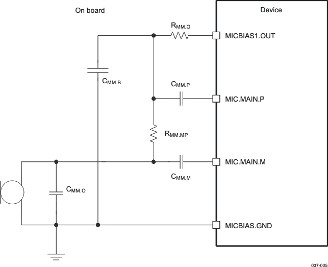 Figure 6-6 Analog Microphone Pseudodifferential
NOTE
For other component values, see Table 5-48.
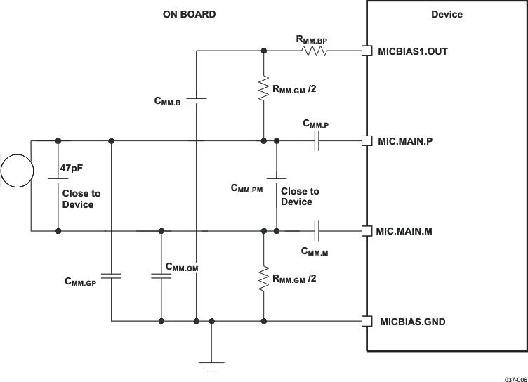 Figure 6-7 Analog Microphone Differential
NOTE
For other component values, see Table 5-48.
NOTE
To improve the rejection, ensure that MICBIAS_GND is as clean as possible. This ground must be shared with AGND of the TPS65920 or TPS65930 device and must not share with AVSS4, which is the ground used by RX class AB output stages.
In differential mode, adding a low-pass filter (made by RSB and CB) is highly recommended if coupling between RX output stages and the microphone is too high (and not enough attenuation by the echo cancellation algorithm). The coupling can come from:
- The internal TPS65920/TPS65930 coupling between MICBIAS.OUT voltage and RX output stages
- Coupling noise between MICBIAS.GND and AVSS4
In pseudodifferential mode, the dynamic resistance of the microphone improves the rejection versus MICBIAS.OUT:
PSRR = 20*log((RB + RDyn_mic)/RB).
6.2.1.2 Silicon Microphone Module Characteristics
Based on silicon micro-electrical-mechanical system (MEMS) technology, the new microphone achieves the same acoustic and electrical properties as conventional microphones, but is more rugged and exhibits higher heat resistance. These properties offer designers of a wide range of products greater flexibility and new opportunities to integrate microphones.
The silicon microphone is the integration of mechanical elements and electronics on a common silicon substrate through microfabrication technology.
The complementary metal oxide semiconductor (CMOS) MEMS microphone is more like an analog IC than a classical microphone, or electric condenser microphone (ECM). It is powered as an IC with a direct connection to the power supply. The on-chip isolation between the power input and the rest of the system adds power supply rejection (PSR) to the component. This makes the CMOS MEMS microphone inherently more immune to power supply noise than an ECM and eliminates the need for additional filtering circuitry to keep the power supply line clean.
Table 6-9 lists the characteristics of the silicon microphone module.
Table 6-9 Silicon Microphone Module Characteristics
| PARAMETER | TEST CONDITIONS | MIN | TYP | MAX | UNIT |
|---|---|---|---|---|---|
| Bias voltage | 2.2 | V | |||
| Load current | 1 | mA | |||
| Output noise | P-weighted 20 Hz to 6.6 kHz | 1.8 | μVRMS |
Figure 6-8 is a schematic for the silicon microphone.
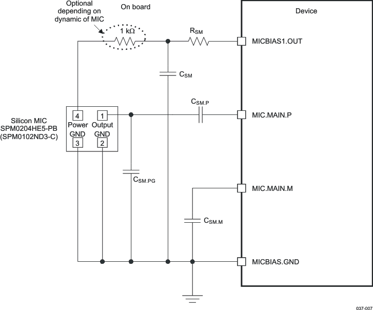 Figure 6-8 Silicon Microphone
NOTE
For other component values, see Table 5-48.
6.2.2 FM Radio/Auxiliary Input
The auxiliary input AUXR/FMR can be used as FM radio input. The amplification stage output is connected to the ADC input. The FM radio input can also be output through an audio output stage.
6.2.2.1 External Components
Figure 6-9 shows the external components on the auxiliary input.
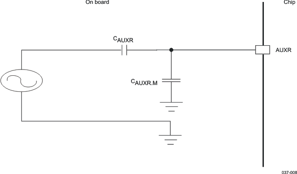 Figure 6-9 Audio Auxiliary Input
NOTE
For other component values, see Table 5-48.
6.2.3 Uplink Characteristics
Figure 6-10 shows the uplink amplifier. Table 6-10 lists the uplink characteristics.
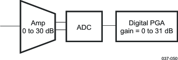 Figure 6-10 Uplink Amplifier
Table 6-10 Uplink Characteristics
| PARAMETER | TEST CONDITIONS | MIN | TYP | MAX | UNIT |
|---|---|---|---|---|---|
| Speech delay | Voice path | 0.5 | ms | ||
| Gain range(1) | 0 | 61 | dB | ||
| Absolute gain | 0 dBFs at 1.02 kHz | –1 | 1 | dB | |
| Peak-to-peak differential input voltage (0 dBFs) | For differential input 0 dB gain setting |
1.5 | VPP | ||
| Peak-to-peak single-ended input voltage (0 dBFs) | For single-ended input 0 dB gain setting |
1.5 | VPP | ||
| Input impedance(2) | 40k | 70k | Ω | ||
| Total harmonic distortion (sine wave at 1.02 kHz) | At –1 dBFs | –80 | –75 | dB | |
| At –6 dBFs | –74 | –69 | |||
| At –10 dBFs | –70 | –65 | |||
| At –20 dBFs | –60 | –55 | |||
| At –60 dBFs | –20 | –15 | |||
| Idle channel noise | 20 Hz to 20 kHz, A-weighted, gain = 0 dB | –85 | –78 | dBFs | |
| 16 kHz: < 20 Hz to 7 kHz, gain = 0 dB | –90 | ||||
| 8 kHz: P-weighted voice, gain = 18 dB | –87 | ||||
| 16 kHz: < 20 Hz to 7 kHz, gain = 18 dB | –82 | ||||
| Crosstalk A/D to D/A | Gain = 0 dB | –80 | dB | ||
| Crosstalk path between two microphones | –70 | dB | |||
| Intermodulation distortion | 2-tone method | –60 | dB |
6.2.4 Microphone Amplification Stage
The microphone amplification stages perform the single-to-differential conversion for single-ended inputs. Two programmable gains from 0 dB to 30 dB can be set:
- Automatic level control for main microphone input. The gain step is 1 dB.
- Level control by register for line-in or carkit input. The gain step is 6 dB.
The amplification stage outputs are connected to the ADC input (ADC left and right).
6.2.5 Carkit Input
The USB-CEA carkit uses the DP pad to input the audio signal.
Figure 6-11 shows the uplink carkit full path uplink characteristics for audio and USB.
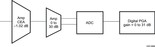 Figure 6-11 Carkit Input Uplink Path Characteristics
Table 6-11 lists the USB-CEA carkit audio electrical characteristics.
Table 6-11 USB-CEA Carkit Audio Uplink Electrical Characteristics
| PARAMETER | TEST CONDITIONS | MIN | TYP | MAX | UNIT |
|---|---|---|---|---|---|
| Gain range (1) | –1 | 60 | dB | ||
| Absolute gain, 0 dBFs at 1.02 kHz (1)(2) | USB-CEA default gain setting | –1.5 | 1.5 | dB | |
| Speech delay | Voice path | 0.5 | ms | ||
| Input common mode voltage (3) | USB-CEA | 1.3 | 1.9 | V | |
| Phone microphone amplifier input impedance at 1 kHz | USB-CEA | 8 | 120 | kΩ | |
| Peak-to-peak single-ended input voltage (0 dBFs) | Default setting | 1.414 | VPP | ||
| Total harmonic distortion (sine wave at 1 kHz), default gain setting | At –1 dBFs | –74 | –60 | dB | |
| At –6 dBFs | |||||
| At –10 dBFs | |||||
| At –20 dBFs | |||||
| At –60 dBFs | |||||
| THD+N (20 Hz to 20 kHz, A-weighted) | At 0 dBFs | 60 | dB | ||
| Signal noise ratio (20 Hz to 20 kHz, A-weighted) | At 0 dBFs | 60 | dB | ||
| Idle channel noise (20 Hz to 20 kHz, A-weighted), default gain setting | USB-CEA | –77 | dBFs | ||
| Output PSRR (20 Hz to 20 kHz, A-weighted) | USB-CEA | 50 | dB |
6.2.6 Digital Audio Filter Module
Figure 6-12 shows the digital audio filter uplink full path characteristics for the audio interface.
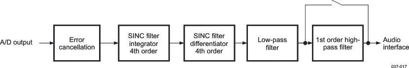 Figure 6-12 Digital Audio Filter Uplink Path Characteristics
The high-pass filter (HPF) can be bypassed. It is controlled by the MISC_SET_2 ATX_HPF_BYP bit set to address 0x49.
Table 6-12 lists the audio filter frequency responses relative to reference gain at 1 kHz.
Table 6-12 Digital Audio Filter TX Electrical Characteristics
| PARAMETER | TEST CONDITIONS | MIN | TYP | MAX | UNIT |
|---|---|---|---|---|---|
| Passband | 0.0005 | 0.42 | FS | ||
| Passband gain | In region 0.0005*FS to 0.42*FS(1) | –0.25 | 0.25 | dB | |
| Stopband | 0.6 | FS | |||
| Stopband attenuation | In region 0.6*FS to 1*FS(1) | 60 | dB | ||
| Group delay | 15.8/FS | μs |