SGLS272I october   2004  – may 2023 TPS715-Q1

PRODUCTION DATA  

  1.   1
  2. Features
  3. Applications
  4. Description
  5. Revision History
  6. Pin Configuration and Functions
  7. Specifications
    1. 6.1 Absolute Maximum Ratings
    2. 6.2 ESD Ratings
    3. 6.3 Recommended Operating Conditions
    4.     Thermal Information
    5. 6.4 Electrical Characteristics
    6. 6.5 Typical Characteristics
  8. Detailed Description
    1. 7.1 Overview
    2. 7.2 Functional Block Diagrams
    3. 7.3 Feature Description
      1. 7.3.1 Wide Supply Range
      2. 7.3.2 Low Quiescent Current
      3. 7.3.3 Dropout Voltage (VDO)
      4. 7.3.4 Current Limit
    4. 7.4 Device Functional Modes
      1. 7.4.1 Normal Operation
      2. 7.4.2 Dropout Operation
  9. Application and Implementation
    1. 8.1 Application Information
    2. 8.2 Typical Application
      1. 8.2.1 Detailed Design Procedure
        1. 8.2.1.1 Programming the TPS71501-Q1 Adjustable LDO Regulator
        2. 8.2.1.2 External Capacitor Requirements
        3. 8.2.1.3 Input and Output Capacitor Requirements
        4. 8.2.1.4 Reverse Current
        5. 8.2.1.5 Feed-Forward Capacitor (CFF)
        6. 8.2.1.6 Power Dissipation (PD)
        7. 8.2.1.7 Estimating Junction Temperature
      2. 8.2.2 Application Curves
    3. 8.3 Power Supply Recommendations
    4. 8.4 Layout
      1. 8.4.1 Layout Guidelines
        1. 8.4.1.1 Power Dissipation
      2. 8.4.2 Layout Example
  10. Device and Documentation Support
    1. 9.1 Device Support
      1. 9.1.1 Development Support
        1. 9.1.1.1 Evaluation Module
        2. 9.1.1.2 Spice Models
      2. 9.1.2 Device Nomenclature
    2. 9.2 Documentation Support
      1. 9.2.1 Related Documentation
    3. 9.3 Receiving Notification of Documentation Updates
    4. 9.4 Support Resources
    5. 9.5 Trademarks
    6. 9.6 Electrostatic Discharge Caution
    7. 9.7 Glossary
  11. 10Mechanical, Packaging, and Orderable Information

Package Options

Refer to the PDF data sheet for device specific package drawings

Mechanical Data (Package|Pins)
  • DCK|5
Thermal pad, mechanical data (Package|Pins)
Orderable Information

Typical Characteristics

GUID-93287514-46B8-4879-BB85-CD91CA481165-low.gif
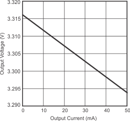
VIN = 4.3 V, COUT = 1 μF, TJ = 25°C
Figure 6-1 Output Voltage vs Output Current for Legacy Chip
GUID-1EC30C8C-BB21-451B-9006-2E3B2EFABEF8-low.gif
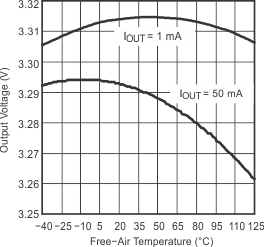
VIN = 4.3 V, COUT = 1 µF
Figure 6-3 Output Voltage vs Free-Air Temperature for Legacy Chip
GUID-9AE050FD-7B46-4542-8ECD-09965F5481EC-low.gif
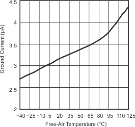
VIN = 4.3 V, VOUT = 3.3 V, IOUT = 1 μF
Figure 6-5 Quiescent Current vs Free-Air Temperature for Legacy Chip
GUID-92FA9D16-21A5-4837-A969-8B363CC6CC10-low.gif
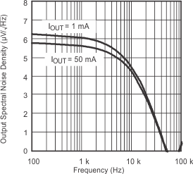
VIN = 4.3 V, VOUT = 3.3 V, COUT = 1 μF
Figure 6-7 Output Spectral Noise Density vs Frequency for Legacy Chip
GUID-E50440EB-E848-4DD3-9705-943721F7B0AE-low.gif
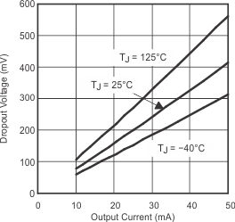
VIN = 3.2 V, COUT = 1 μF
Figure 6-9 Dropout Voltage vs Output Current for Legacy Chip
GUID-32F2D415-E96B-4083-AF69-C0D85E512B49-low.gif
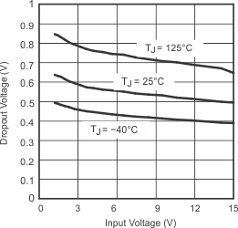
IOUT = 50 mA
Figure 6-11 TPS71501 Dropout Voltage vs Input Voltage for Legacy Chip
GUID-8A896593-541F-425B-9977-DF620F72CAD0-low.gif
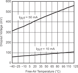
VIN = 3.2 V
Figure 6-13 Dropout Voltage vs Free-Air Temperature for Legacy Chip
GUID-5C279F69-E588-45B0-B1E6-FE30E07A4435-low.gif
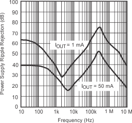
VIN = 4.3 V, VOUT = 3.3 V, COUT = 10 μF, TJ = 25°C
Figure 6-15 Power-Supply Ripple Rejection vs Frequency for Legacy Chip
GUID-DD9F7269-9C5B-46E8-879D-2A419464AD08-low.gif
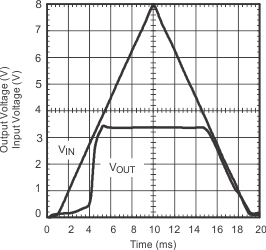
VOUT = 3.3 V, RL = 66 Ω, COUT = 10 μF
Figure 6-17 Power-Up and Power-Down for Legacy Chip
GUID-EEBD61C9-3179-477E-90E7-EAEB17D31F8F-low.gif
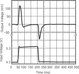
VOUT = 3.3 V, IOUT = 50 mA, COUT = 10 μF
Figure 6-19 Line Transient Response for Legacy Chip
GUID-26F0C422-F6D0-4A72-8A97-CF2927027251-low.gif
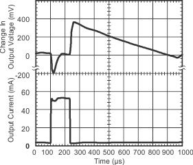
VIN = 4.3 V, VOUT = 3.3 V, COUT = 10 μF
Figure 6-21 Load Transient Response for Legacy Chip
GUID-1DC91A95-FA05-4DD0-A225-F272AF91EC5C-low.gif
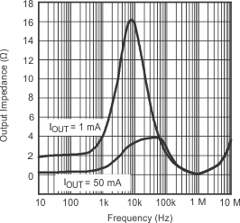
VIN = 4.3 V, VOUT = 3.3 V, COUT = 1 μF, TJ = 25°C
Figure 6-23 Output Impedance vs Frequency for Legacy Chip
GUID-3F8F7029-4114-407E-80A7-A76A5165B7B3-low.svg
VIN = 4.3 V, COUT = 1 μF, TJ = 25°C
Figure 6-2 Output Voltage vs Output Current for New Chip
GUID-BC339FCB-4CC8-4E33-A7C1-BA1F033C8378-low.svg
VIN = 4.3 V, COUT = 1 µF
Figure 6-4 Output Voltage vs Free-Air Temperature for New Chip
GUID-9530ABE3-1507-4146-B53F-01F3684FCA51-low.svg
VIN = 4.3 V, VOUT = 3.3 V, COUT = 1 μF
Figure 6-6 Quiescent Current vs Free-Air Temperature for New Chip
GUID-B89DCE2F-6120-4F8A-BC3D-364858D07BF6-low.svg
VIN = 4.3 V, VOUT = 3.3 V, COUT = 1 μF
Figure 6-8 Output Spectral Noise Density vs Frequency for New Chip
GUID-B3E34136-2E8E-4881-8719-4AEC45252A8B-low.svg
VIN = 3.2 V, COUT = 1 μF
Figure 6-10 Dropout Voltage vs Output Current for New Chip
GUID-DF877B52-FFD0-4F33-A727-5E299F64B6EF-low.svg
IOUT = 50 mA
Figure 6-12 TPS71501 Dropout Voltage vs Input Voltage for New Chip
GUID-9E304323-3AEE-49B2-A33B-B793AE118DF2-low.svg
VIN = 3.2 V
Figure 6-14 Dropout Voltage vs Free-Air Temperature for New Chip
GUID-0B50574A-73C5-43CC-88E4-3F2F581CB86C-low.svg
VIN = 4.3 V, VOUT = 3.3 V, COUT = 10 μF, TJ = 25°C
Figure 6-16 Power-Supply Ripple Rejection vs Frequency for New Chip
GUID-96DBF883-59F3-4C30-9A18-EE0299DD7951-low.svg
VOUT = 3.3 V, RL = 66 Ω, COUT = 10 μF
Figure 6-18 Power-Up and Power-Down for New Chip
GUID-C811A98F-8373-4637-9429-CBDCE6D87402-low.svg
VOUT = 3.3 V, IOUT = 50 mA, COUT = 10 μF
Figure 6-20 Line Transient Response for New Chip
GUID-7C092A47-6F6F-4A9C-A124-33610EC1EAB0-low.svg
VIN = 4.3 V, VOUT = 3.3 V, COUT = 10 μF
Figure 6-22 Load Transient Response for New Chip